

Silicon integrated circuit operating at microwave frequencies and fabrication process
a technology of integrated circuits and microwave frequencies, applied in the direction of resistors, electrical devices, solid-state devices, etc., can solve the problems of low resistivity of silicon or germanium substrates, unfavorable propagation of signals, and substrates that are source of transmission losses, so as to reduce propagation losses
- Summary
- Abstract
- Description
- Claims
- Application Information
AI Technical Summary
Benefits of technology
Problems solved by technology
Method used
Image

Examples
Embodiment Construction
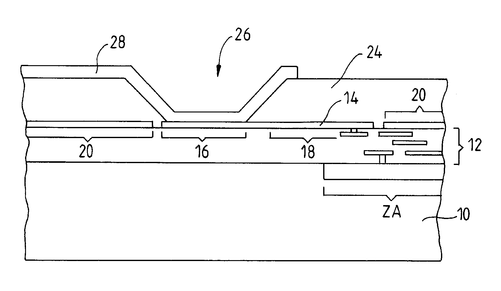
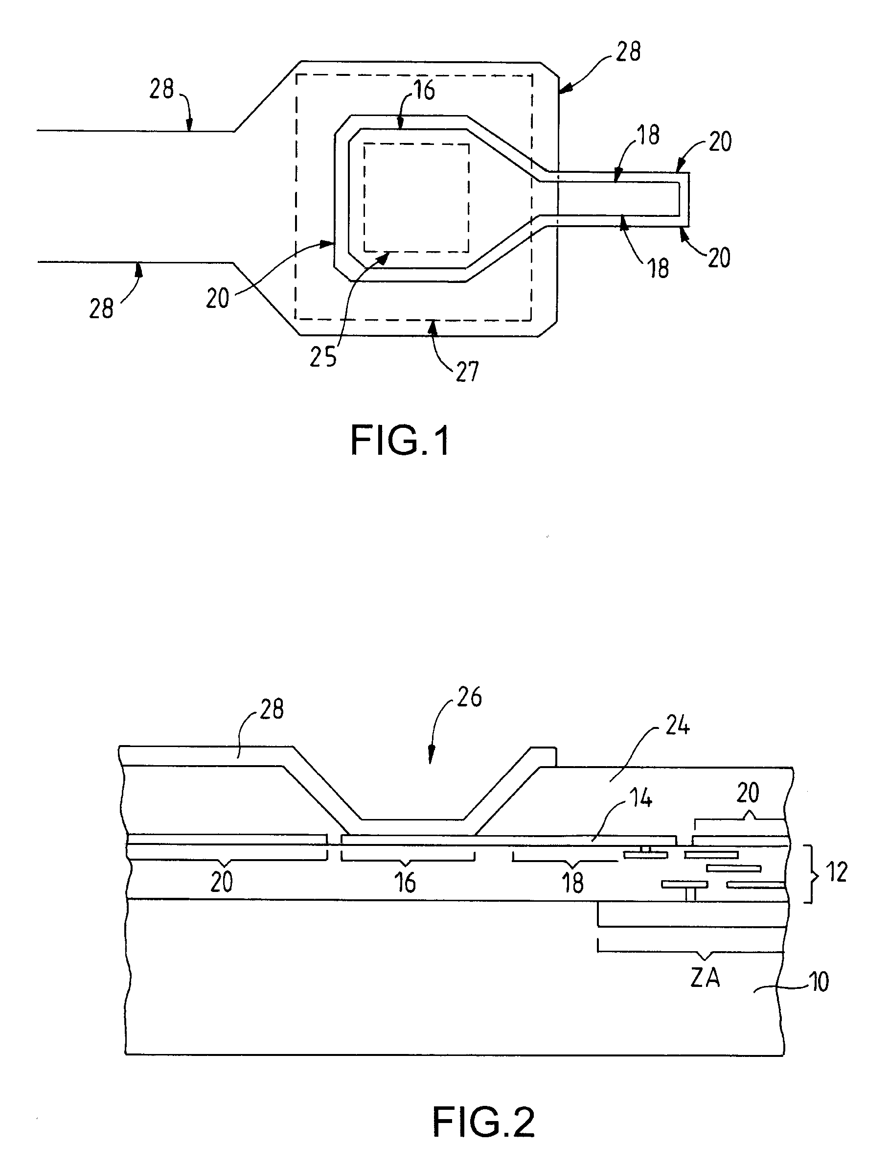
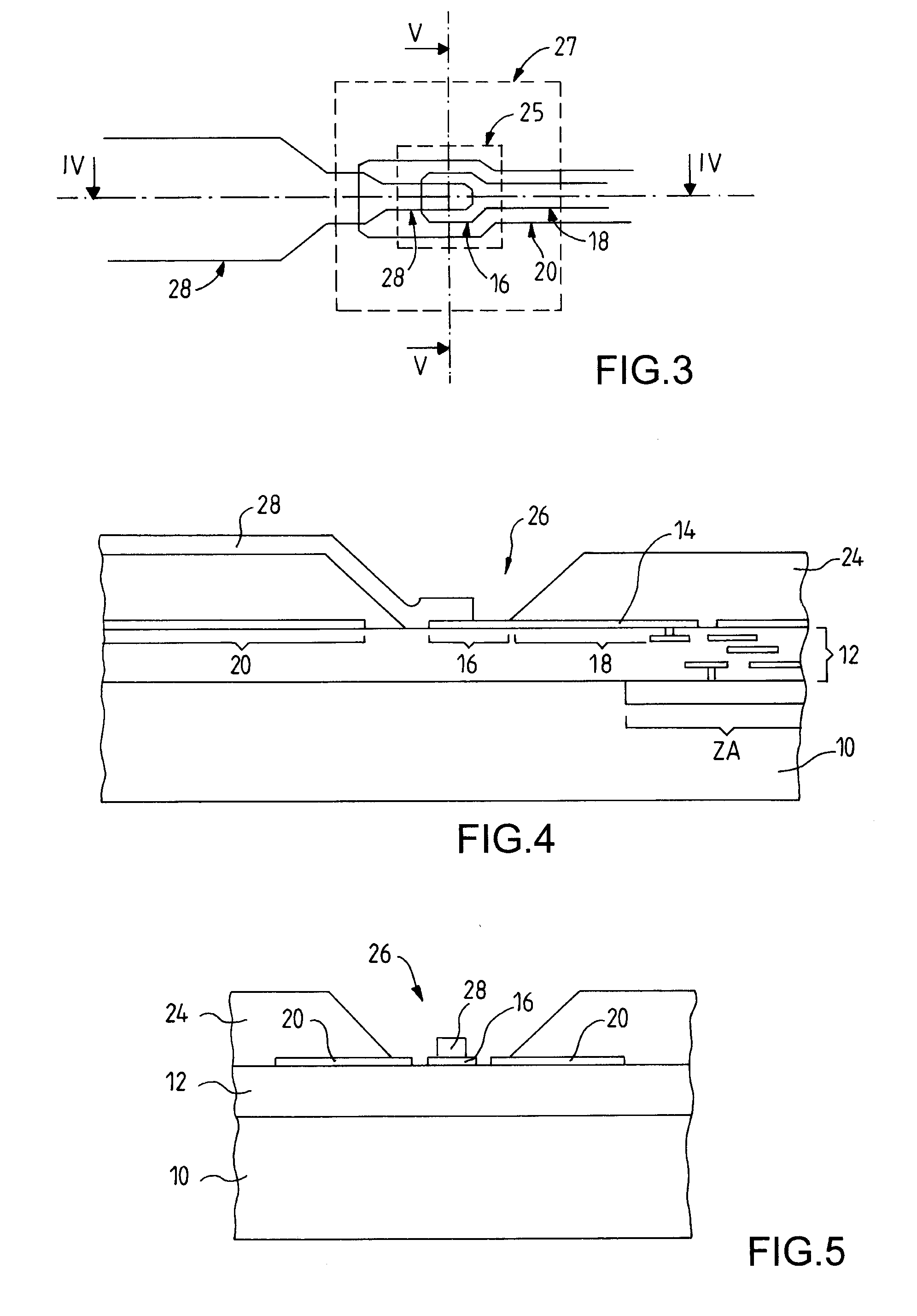
[0025]FIGS. 1 and 2 are described together. The microwave integrated circuit is produced on a main face (front face) of a silicon substrate 10. The substrate could also be made of germanium, but in the rest of the description silicon will be considered, which is a more advantageous material from the standpoint of industrial control of its use. The active or passive elements of this circuit are formed in an active zone denoted by the reference ZA (FIG. 2), which comprises both active or passive elements and interconnections over several metallic levels. The active elements are essentially transistors. The interconnection layers internal to the integrated circuit are produced by metallic levels (made of aluminum in general) embedded in insulating layers, which are usually made of silicon oxide. The various levels are connected together by conducting vias. The overall insulating layer incorporating these various metallic interconnection levels and the connection vias is denoted by the ...
PUM
 Abstract
Description
Claims
Application Information