System for checking clock-signal correspondence

Active Publication Date: 2007-11-01
ARM LTD
View PDF9 Cites 19 Cited by
  • Summary
  • Abstract
  • Description
  • Claims
  • Application Information

AI Technical Summary

Benefits of technology

[0038] In one embodiment the transition generator is operable to generate the perturbation in the transition signal such that a transition occurs substantially coincident with an active edge of said further clock signal such that it has opposite polarity to the most recent preceding transition that was substantially coincident with an active edge of said further clock signal and the level of said transition signal at any intervening active edges of said further clock signal that were not substantially coincident with a transition in said transition signal did not cause a change in the output of the further signal path.
[0039] In one embodiment the perturbation an the transition signal is controlled in dependence upon at least one of (i) information with regard to expected timings of clock edges of the further clock and (ii) feedback from the further clock signal indicating timings of clock edges of the further clock. This enables the timing of the perturbation and of the transitions in the transition

Problems solved by technology

However, it is difficult, for example, to generate clocks which are integer divisions of each other frequencies while maintaining low skew between the output clocks.
In particular, there is no “clock re-synthesis” or clock balancing included in the known FPGA tools to support this.
However, such static timing analysis tools are not capable of analysing clock paths that are external to an FPGA such as clock paths that are involved in generation and distribution of the clocks via board-level components before those clocks are passed into the FPGA.
Although it is possible to explicitly place circuit el

Method used


Image

  • System for checking clock-signal correspondence
  • System for checking clock-signal correspondence
  • System for checking clock-signal correspondence

Examples


Example

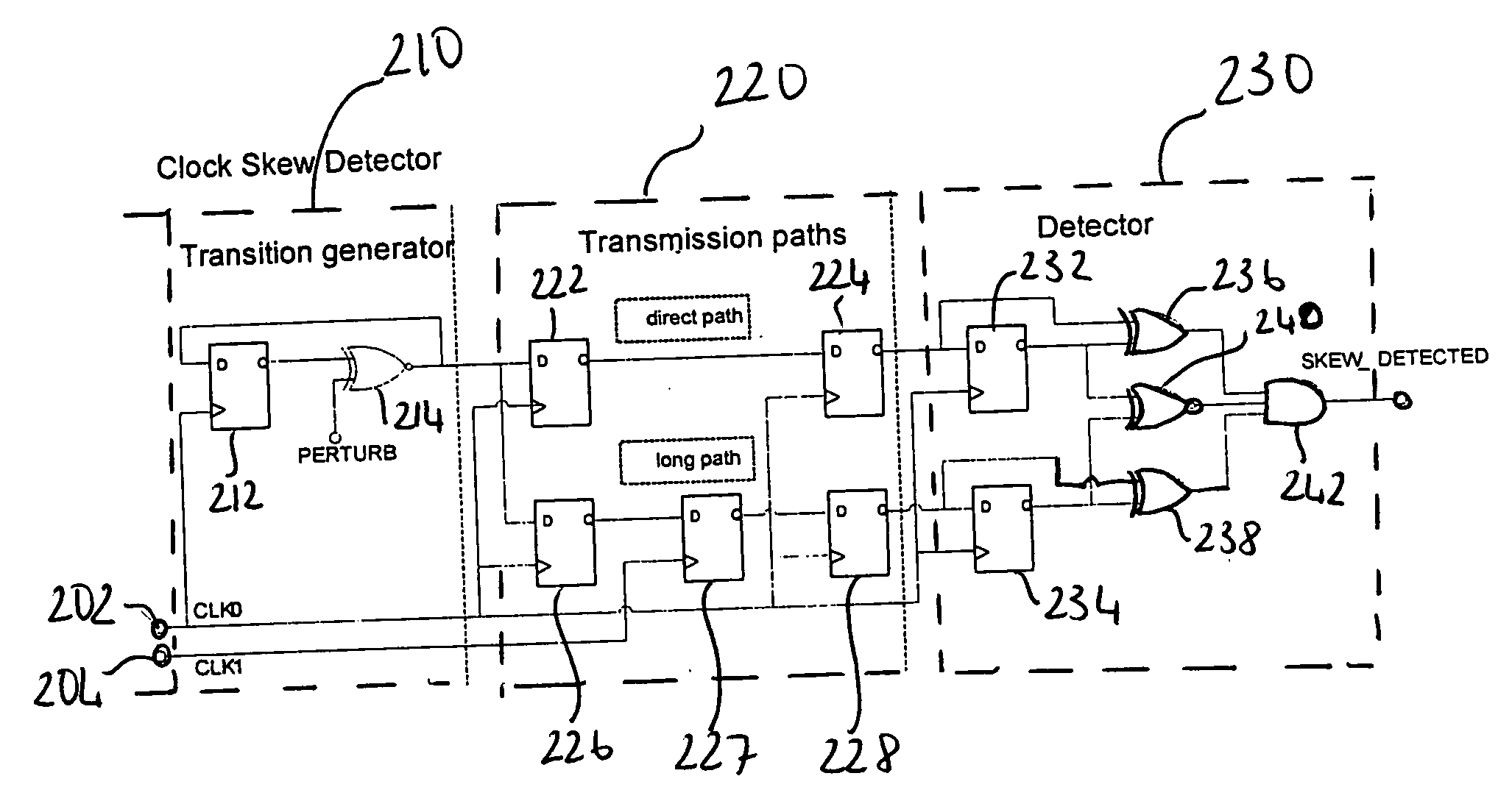
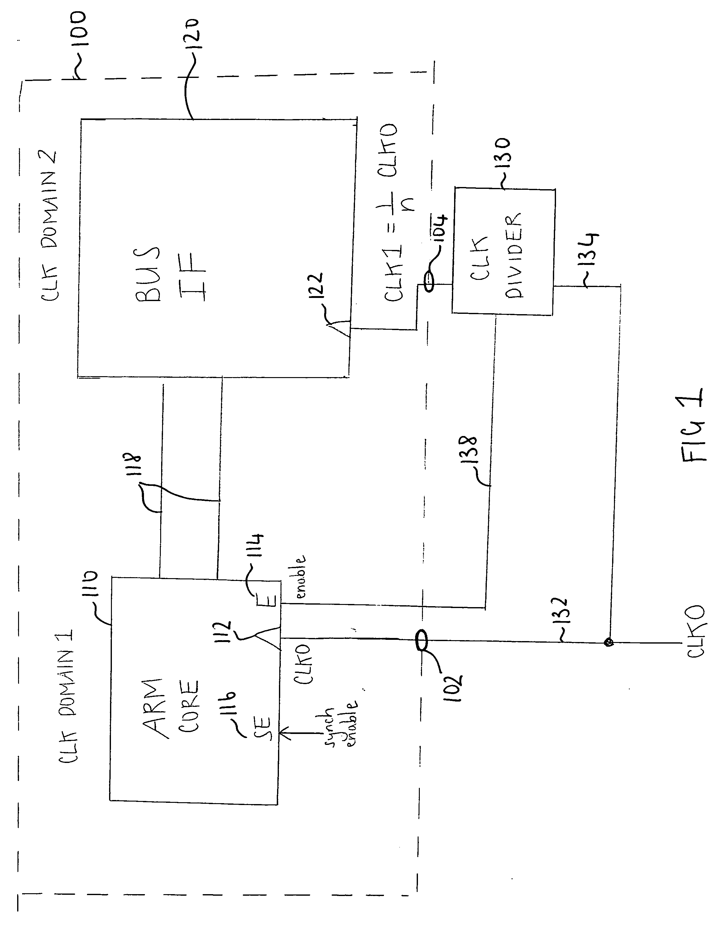
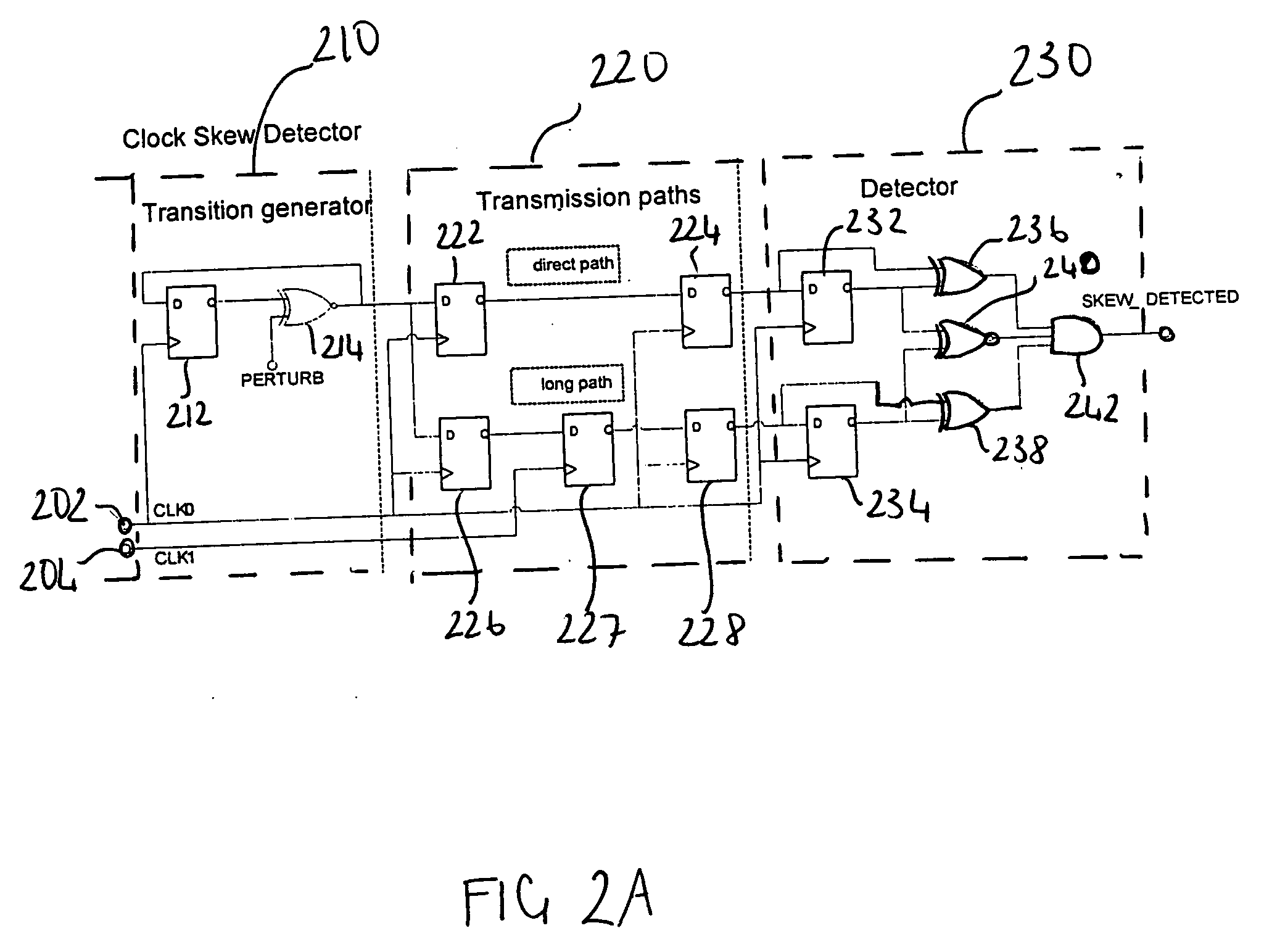
[0102]FIG. 1 schematically illustrates a programmable logic device having more than one clock domain. The system comprises a programmable logic device having an ARM processor core 110 and a bus interface circuit 120 and a clock divider 130, which is situated externally to the programmable logic device. The ARM core 110 and the bus interface 120 communicate via a pair of signal lines 118.

[0103] The ARM core 110 has a clock signal input 112, an enable input 114 and a synchronisation (sync) enable input 116. A reference clock signal CLK0 is supplied directly to the clock signal input 112 of the ARM core via a signal line 132. CLK0 is also supplied to the clock divider 130 via the signal line 134. The external clock divider 130 reduces the frequency of the reference clock signal CLK0 (divides frequency by a non-zero integer) and outputs a further (lower frequency) clock signal CLK1 via the signal line 104 to the clock input 122 of the bus interface 120. Thus the ARM core 110 is clocked...


PUM


Abstract

A data processing system is provided having a clock signal comparator comprising a reference input port for receiving a reference clock signal and at least a further input port for receiving respective further clock signal. Checking logic is provided within the clock signal comparator to check for a correspondence between the clock edge of the reference clock signal and a corresponding clock edge of the further clock signal within a predetermined time window. The checking logic is operable to check for the correspondence during operation of the data processing system. The clock-signal comparator can be provided on an integrated circuit or as part of the data processing apparatus having at least two different timing domains such as timing domains associated with two different instances of the same clock. Furthermore the clock-signal comparator is implemented in a hardware description language and integrated in a simulation of the operation of a data processing apparatus to detect timing errors that arise from numerical artefacts of the simulation as well as timing errors that arise from configuration and layout of the circuit elements of the data processing apparatus being simulated.

Description

BACKGROUND OF THE INVENTION [0001] 1. Field of the Invention [0002] This invention relates to the field of data processing systems. More particularly, this invention relates to checking for correspondence between clock signals. [0003] 2. Description of the Prior Art [0004] It is known to provide data processing systems such as integrated circuits having processing logic that is sub-divided into several clock domains which require gated or different frequency clocks to be generated and distributed with controlled “clock skew” between them to allow signals to pass between the different clock domains without timing violations. Clock skew is defined herein to be a situation where corresponding rising and / or falling edges of two different clock signals are non-coincident. [0005] It is known in systems such as Field Programmable Gate Arrays (FPGA) to provide a number of low skew global clock buffers with similar distribution insertion delays. However, it is difficult, for example, to gene...

Claims


Application Information

Patent Timeline
IPC IPC(8): G06F1/04
CPCH03K23/52G06F1/10
Inventor GILDAY, DAVID MICHAELBRADLEY, DARYL WAYNEASHFIELD, EDMOND JOHN SIMON
Owner ARM LTD
Why Eureka
Try Eureka