Field-effect transistor

a field-effect transistor and transistor technology, applied in transistors, semiconductor devices, electrical equipment, etc., can solve the problems of overcurrent flow between source and drain, destroying fet itself,

Inactive Publication Date: 2007-11-29
SHARP KK
View PDF4 Cites 9 Cited by
  • Summary
  • Abstract
  • Description
  • Claims
  • Application Information

AI Technical Summary

Benefits of technology

[0027]According to the present invention, it is possible to provide a normally-off type FET including a heterostructure of nitride semiconductor layers.

Problems solved by technology

On the other hand, in the use of the normally-on type, when gate voltage Vg becomes zero for some reasons, overcurrent flows between source and drain, possibly destroying FET itself.

Method used


Image

  • Field-effect transistor
  • Field-effect transistor
  • Field-effect transistor

Examples


first embodiment

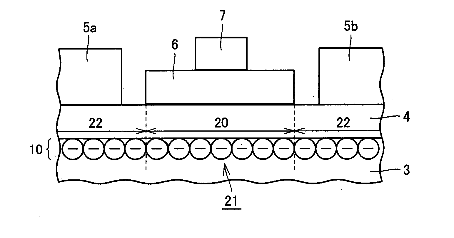
[0043]FIG. 1 is a schematic cross-sectional view of a preferable example of FET in accordance with the present invention. Here, FET of the present invention has a structure in which a buffer layer 2 formed of AlN, a first nitride semiconductor layer 3 formed of GaN, and a second nitride semiconductor layer 4 formed of Al0.3Ga0.7N are stacked on a semiconductor substrate 1 formed of SiC in the c-axis direction in this order by hetero-epitaxial growth. A source electrode 5a is formed on one end of a surface of second nitride semiconductor layer 4 and a drain electrode 5b is formed on the other end thereof. Furthermore, a piezo-effect film 6 having a piezo effect is formed on a region of the surface of second nitride semiconductor layer 4 between source electrode 5a and drain electrode 5b, and a gate electrode 7 is formed on a region of a surface of piezo-effect film 6.

[0044]Here, first nitride semiconductor layer 3 formed of GaN has a lattice constant a1 and a bandgap Eg1 (a1=3.189 Å,...

second embodiment

[0057]FIG. 5 shows a schematic cross-sectional view of another preferable example of FET in accordance with the present invention. Here, FET of the present invention has a structure in which a buffer layer 12 formed of AlN, a first nitride semiconductor layer 13 formed of Al0.3Ga0.7N, and a second nitride semiconductor layer 14 formed of GaN are stacked on a semiconductor substrate 11 formed of SiC in the c-axis direction in this order by hetero-epitaxial growth. Source electrode 5a is formed on one end of a surface of second nitride semiconductor layer 14 and drain electrode 5b is formed on the other end thereof. Furthermore, piezo-effect film 6 having a piezo effect is formed on a region of the surface of second nitride semiconductor layer 14 between source electrode 5a and drain electrode 5b, and gate electrode 7 is formed on a region of a surface of piezo-effect film 6.

[0058]Here, first nitride semiconductor layer 13 formed of Al0.3Ga0.7N has a lattice constant a1 and a bandgap ...

example 1

[0086]FET of Example 1 having the cross-sectional structure shown in FIG. 1 was fabricated. In fabrication of this FET, first, buffer layer 2 (20 nm thick) formed of AlN was grown on an Si atomic plane of semiconductor substrate 1 formed of SiC with the temperature of semiconductor substrate 1 of 1200° C. by MOCVD (metal organic chemical vapor deposition). Then, with the temperature of semiconductor substrate 1 of 1100° C., first nitride semiconductor layer 3 formed of GaN (lattice constant a1=3.189 Å, Eg1=3.42 eV) was grown to a thickness of 3 μm. With the temperature of semiconductor substrate 1 of 1100° C., second nitride semiconductor layer 4 formed of Al0.3Ga0.7N (a2=3.166 Å, Eg2=4.02 eV) was grown thereon to a thickness of 20 nm.

[0087]Thereafter, in order to form source electrode 5a and drain electrode 5b, a resist is patterned using a photolithography method, and an Hf film (10 nm thick) / an Al film (100 nm thick) / an Hf film (40 nm thick) / an Au film (240 nm thick) were then st...


PUM


Abstract

A field-effect transistor is provided which includes: a first nitride semiconductor layer having a lattice constant a1 and a bandgap Eg1; a second nitride semiconductor layer stacked on the first nitride semiconductor layer and having a lattice constant a2 and a bandgap Eg2; a source electrode and a drain electrode formed on the second nitride semiconductor layer; a piezo-effect film formed on the second nitride semiconductor layer in a region between the source electrode and the drain electrode; and a gate electrode formed on a region of the piezo-effect film. The relation between the lattice constants a1 and a2 is a1>a2. The relation between the bandgaps Eg1 and Eg2 is Eg1<Eg2. The residual polarization density at that surface of the piezo-effect film which faces the second nitride semiconductor layer is equal to or higher than the density of electric charges of a two-dimensional electron gas layer at an interface between the first nitride semiconductor layer and the second nitride semiconductor layer, and negative charges are polarized at that surface of the piezo-effect film which faces the second nitride semiconductor layer.

Description

[0001]This nonprovisional application is based on Japanese Patent Application No. 2006-143069 filed with the Japan Patent Office on May 23, 2006, the entire contents of which are hereby incorporated by reference.BACKGROUND OF THE INVENTION[0002]1. Field of the Invention[0003]The present invention relates to a field-effect transistor (FET) and more particularly a normally-off type FET including a heterostructure of nitride semiconductor layers.[0004]2. Description of the Background Art[0005]A conventional FET using a group III-V compound nitride semiconductor includes a heterostructure of a GaN layer and an AlGaN layer on a substrate (see Patent Document 1: U.S. Pat. No. 5,192,987). Here, the AlGaN layer has a smaller lattice constant than the GaN layer.SUMMARY OF THE INVENTION[0006]In formation of this heterostructure, a thin AlGaN layer having a thickness of, for example, 20 nm is epitaxially grown on a relatively thick GaN layer having a thickness of, for example, 1 μm. Here, the ...

Claims


Application Information

Patent Timeline
Patent Type & Authority Applications(United States)
IPC IPC(8): H01L29/788
CPCH01L29/7787H01L29/2003
Inventor TERAGUCHI, NOBUAKI
Owner SHARP KK
Why Eureka
Try Eureka