

Reflective mask blank, reflective mask, and method of manufacturing semiconductor device
a reflective mask and semiconductor technology, applied in the field of exposure reflective masks, can solve the problems of insufficient oxidation prevention effect, low reflectance, and rapid oxidation of mo, and achieve the effect of preventing oxidation of multi-layer reflective films and excellent environmental resistan
- Summary
- Abstract
- Description
- Claims
- Application Information
AI Technical Summary
Benefits of technology
Problems solved by technology
Method used
Image

Examples
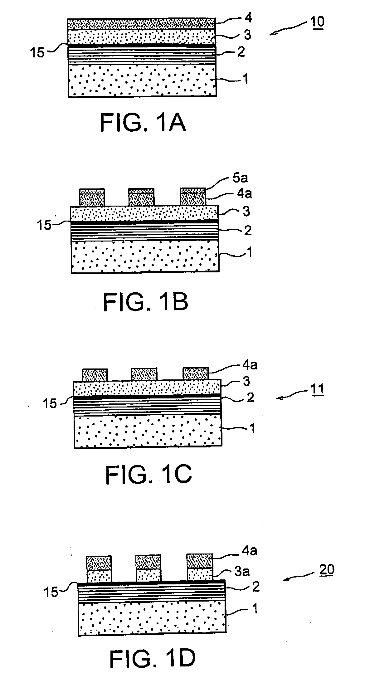
first embodiment
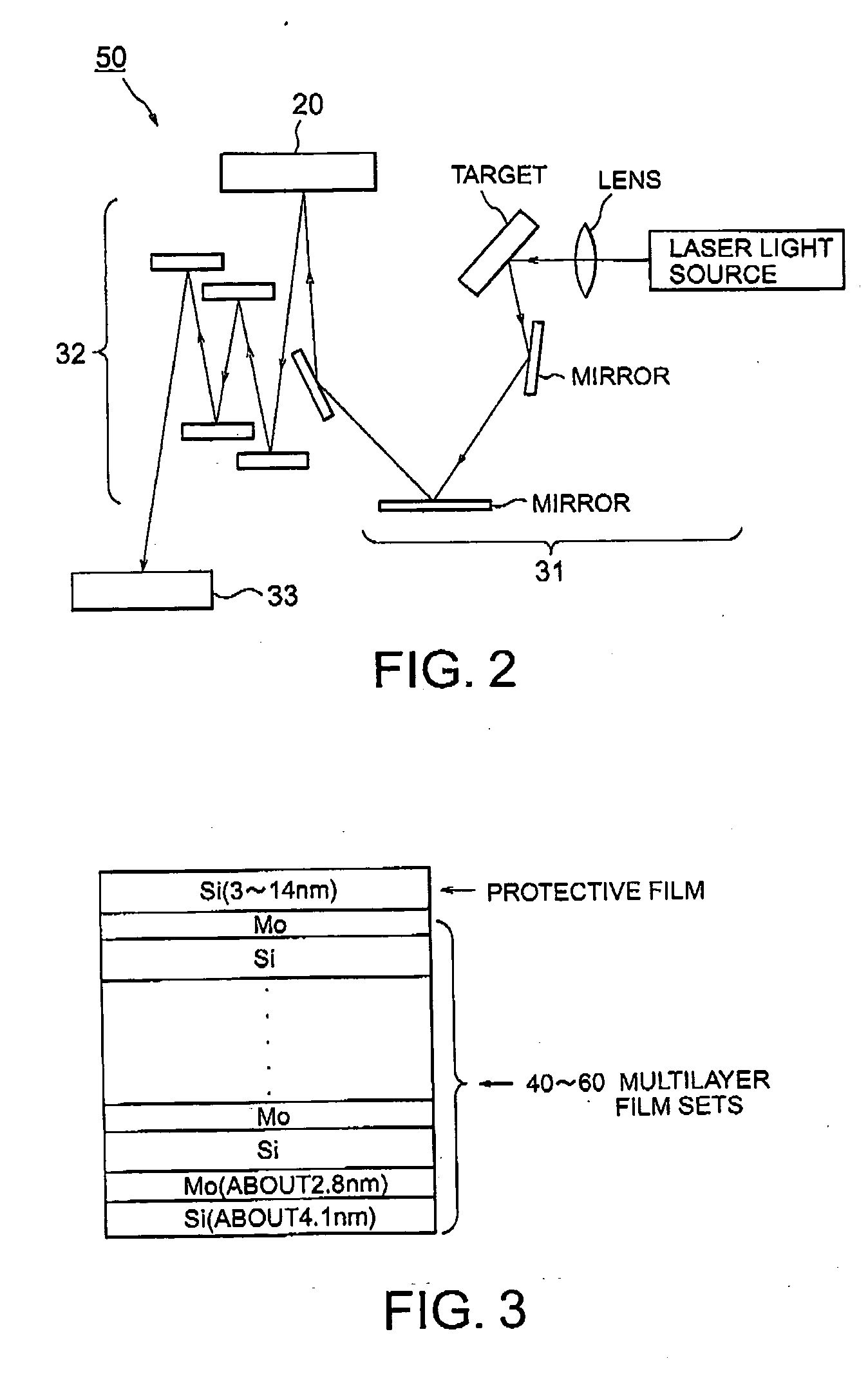
[0046] The protective film according to the first embodiment is specified by a material formed by a ruthenium compound that contains ruthenium (Ru) and an element that may be either molybdenum (Mo) or niobium (Nb).
[0047] As typical materials included in the protective film according to the first embodiment, Mo63Ru37 and NbRu are exemplified.
[0048] By comprising the protective film of the first embodiment, there is obtained a reflective mask blank having the following six effects A to F.
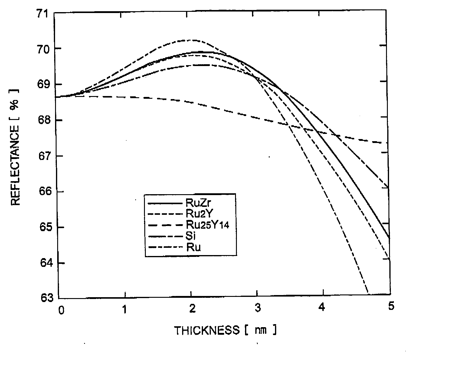
[0049] A. A higher reflectance is obtained as compared with a Ru film or a Si film (capping layer) as an uppermost layer of a multilayer reflective film.
[0050] B. During formation of the protective film, a diffusion layer is hardly formed between the protective film and the Si film placed as the uppermost layer of the multilayer reflective film. Such diffusion might be caused to occur during heat treatment after formation of the protective film (heat treatment for reducing the stress of the multil...
second embodiment
[0055] The protective film according to the second embodiment of this invention is featured by a ruthenium compound that contains ruthenium (Ru) and an element that is either zirconium (Zr) or yttrium (Y).
[0056] As typical materials included in the protective film according to the second embodiment, ZrRu, Ru2Y, and Ru25Y44 can be exemplified.
[0057] By comprising the protective film of the second embodiment, there is obtained a reflective mask blank having the following five effects B to F.
[0058] B. During formation of the protective film, a diffusion layer is hardly formed between the protective film and the Si film placed as the uppermost layer of the multilayer reflective film. Such diffusion might be caused to occur during heat treatment after formation of the protective film (heat treatment for reducing the stress of the multilayer reflective film, prebake treatment of a resist film, cleaning, etc.). Therefore, a reduction in reflectance due to the formation of the diffusion ...
third embodiment
[0063] The protective film according to the third embodiment is featured by a ruthenium compound containing ruthenium (Ru) and an element selected from boron (B), titanium (Ti), and lanthanum (La).
[0064] As typical materials included in the protective film according to the third embodiment, Ru7B3, RuB, Ru2B3, RuB2, TiRu, and LaRu2 can be exemplified.
[0065] By comprising the protective film of the third embodiment, there is obtained a reflective mask blank having the following four effects B, C, D, and F.
[0066] B. During formation of the protective film, a diffusion layer is hardly formed between the protective film and the Si film placed as the uppermost layer of the multilayer reflective film. Such diffusion might be caused to occur during heat treatment after formation of the protective film (heat treatment for reducing the stress of the multilayer reflective film, prebake treatment of a resist film, cleaning, etc.). Therefore, a reduction in reflectance due to the formation of...
PUM
| Property | Measurement | Unit |
|---|---|---|
| wavelength | aaaaa | aaaaa |
| thickness | aaaaa | aaaaa |
| reflectance | aaaaa | aaaaa |
Abstract
Description
Claims
Application Information