Method of the manufacturing an organic EL display

a manufacturing method and technology of organic el, applied in the manufacture of electrode systems, final products, electric discharge tubes/lamps, etc., can solve the problems of pattern reproducibility, decomposition of color conversion dyes, and actual decrease of efficiency, so as to avoid color conversion layer distortion, shorten manufacturing steps, and high color conversion efficiency

Inactive Publication Date: 2007-11-29
FUJI ELECTRIC CO LTD
View PDF8 Cites 18 Cited by
  • Summary
  • Abstract
  • Description
  • Claims
  • Application Information

AI Technical Summary

Benefits of technology

[0008] It is therefore an object of the present invention to provide a method of manufacturing an organic EL display in which manufacturing processes are simplified and high definition patterning is performed.
[0019] A manufacturing method according to the invention constituted as described above allows forming a color conversion layer with high definition owing to the self-alignment secured by the color filter layers that work as a mask. A color conversion filter with high color conversion efficiency can be achieved by combining the color filter layer and the color conversion layer. Such a method according to a preferred embodiment of the invention eliminates the need for patterning the color conversion layer by means of photolithography or mask evaporation, thereby shortening the manufacturing steps. Since partial regions of a monolithically formed dye layer are converted to the color conversion layers, the color conversion layers and surrounding layers (a transparent layer, for example) can be formed as a monolithic single film. Therefore, distortion of the color conversion layer is avoided even in the case of forming a narrower color conversion layer than the film thickness. Consequently, displays for use in micro displays (for example, a viewing finder in a video camera) can be manufactured by a method according to a preferred embodiment of the invention.

Problems solved by technology

Major practical problems in color displays include, in addition to definite color display performance and long-term stability, reproducibility of color and provision of a color conversion filter exhibiting high color conversion efficiency.
However, if the concentration of the color conversion dye is increased to increase color conversion efficiency, the efficiency actually decreases due to so-called concentration quenching, and decomposition of the color conversion dye occurs with the passage of time.
However, in a case of patterning having a width smaller than a film thickness, for example, problems of reproducibility of the pattern and distortion of the pattern in the subsequent processes may arise.
So, a procedure of producing the full color display requires multiple steps and is rather complicated.
The mask evaporation method, however, requires high precision alignment in a vacuum.
That is a highly difficult process, and limitations exist in the degree of definition and the substrate dimensions that can be employed.

Method used


Image

  • Method of the manufacturing an organic EL display
  • Method of the manufacturing an organic EL display
  • Method of the manufacturing an organic EL display

Examples


example 1

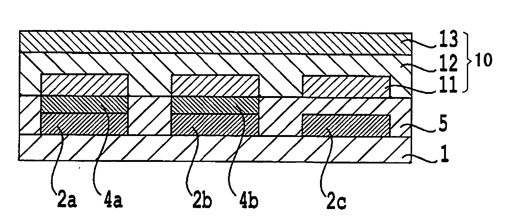
[0101] Blue color filter material (Color Mosaic CB-7001, a product of FUJIFILM Electronic Materials Co., Ltd.) was applied on a transparent glass substrate (Corning 1737 glass) by a spin coating method, and patterned by a photolithography method, to form a blue color filter layer of plural strips extending in the longitudinal direction having a line width of 0.1 mm, a pitch of 0.33 mm (distance between two adjacent lines being 0.23 mm), and a film thickness of 2 μm.

[0102] On the substrate having the blue color filter layer, a green color filter material (Color Mosaic CG-7001, a product of FUJIFILM Electronic Materials Co., Ltd.) was applied by a spin coating method, and patterned by a photolithography method, to form a green color filter layer of plural stripes extending in the longitudinal direction having a line width of 0.1 mm, a pitch of 0.33 mm, and a film thickness of 2 μm.

[0103] Next, a red color filter material (Color Mosaic CR-7001, a product of FUJIFILM Electronic Materi...

example 2

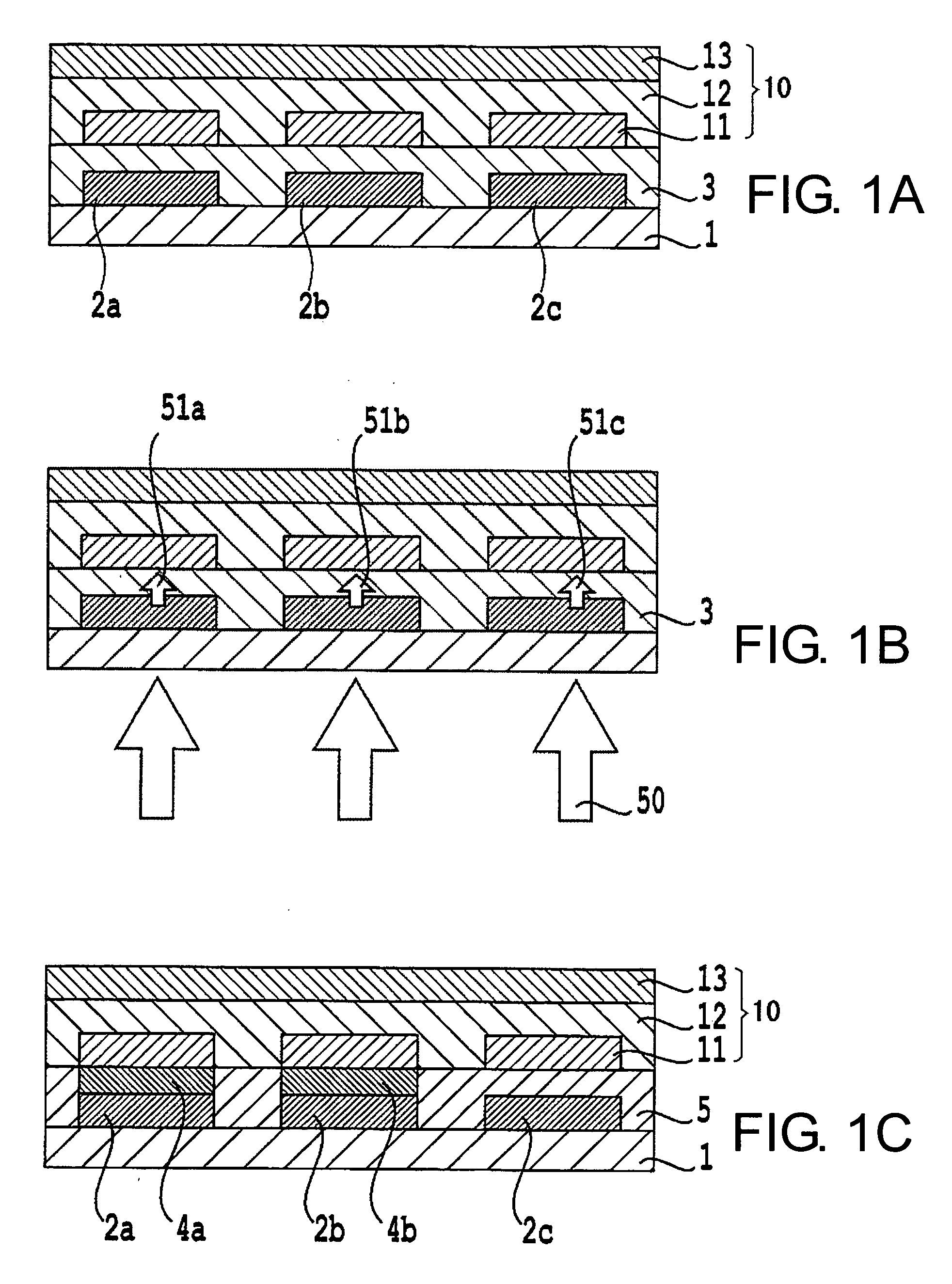
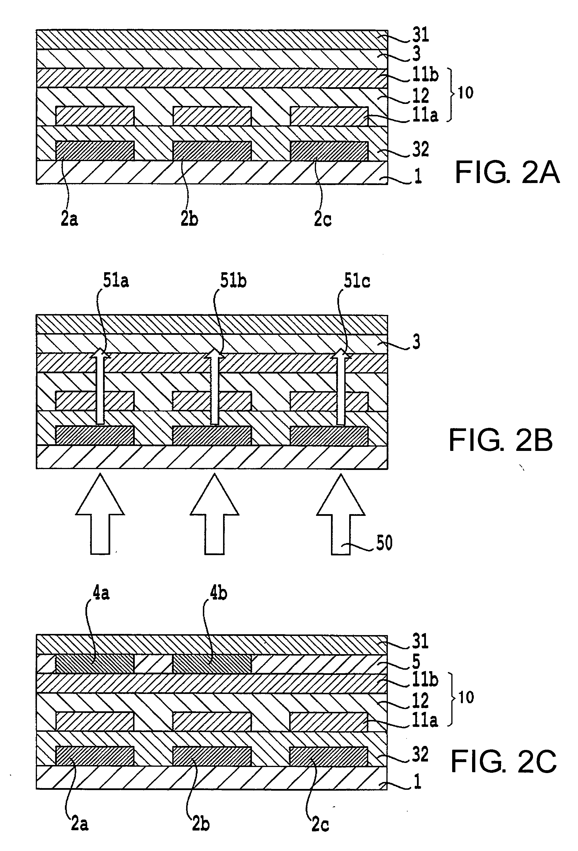
[0111] An organic EL display was manufactured in the same manner as in Example 1 except that a forward bias voltage of 10 V was applied on the organic EL layer, linearly and sequentially scanning the transparent electrode elements and the reflective electrode elements in the process of dye-decomposing light irradiation. In this example, the irradiation time of the dye-decomposing light was shortened by 30% as compared with in Example 1, demonstrating promotion of decomposition of the color conversion dye in the dye layer by the emission from the organic EL layer.

example 3

[0112] An organic EL display was manufactured in the same manner as in Example 2 except that the light emitting elements in the area corresponding to the red color filter layer was not lit in the process of the linear and sequential scanning of the transparent electrode elements and the reflective electrode elements. In this Example, also, as in Example 2, the irradiation time of the dye-decomposing light was shortened by 30% as compared with in Example 1, demonstrating promotion of decomposition of the color conversion dye in the dye layer by the emission from the organic EL layer.


PUM


Abstract

Manufacturing an organic EL display by: forming n types of color filter layers on a transparent substrate; forming a dye layer containing (n−1) types of color conversion dyes by a dry process; forming an organic EL device on the dye layer; and exposing the dye layer to dye-decomposing light from the side of the transparent substrate to form an m-th type color conversion layer at a position corresponding to an m-th type color filter layer; where n represents an integer from 2 to 6; m represents an integer from 1 to (n−1); each of the color filter layers transmits light in a different wavelength region; m-th type color conversion dye is decomposed by light cut by the m-th type color filter layer; and the m-th type color conversion layer emits light transmitted by the m-th type color filter layer after wavelength distribution conversion.

Description

CROSS-REFERENCE TO RELATED APPLICATION [0001] This application is based on, and claims priority to, Japanese Patent Application No. 2005-360975, filed on Dec. 14, 2005, the contents of which are incorporated herein by reference. BACKGROUND OF THE INVENTION [0002] 1. Field of the Invention [0003] The present invention relates to a method of manufacturing an organic EL display capable of multi color display. The organic EL display can be applied, for example, to image sensors, personal computers, word processors, televisions, facsimiles, audio equipment, video recorders, car navigation, electronic calculators, telephones, mobile terminals, and industrial instruments. [0004] 2. Description of the Related Art [0005] For multi color or full color display, color conversion systems have recently been studied that use a filter containing color conversion dye that absorbs light in the near-ultraviolet, blue, blue-green, or white light spectra, changes the wavelength distribution of the light...

Claims


Application Information

Patent Timeline
Patent Type & Authority Applications(United States)
IPC IPC(8): H01J9/24
CPCH01L51/56H01L27/322Y02E10/549Y02P70/50H10K59/38H10K71/00H10K30/82H10K50/84H10K50/11
Inventor KAWAGUCHI, KOJIHAMA, TOSHIOTERAO, YUTAKA
Owner FUJI ELECTRIC CO LTD
Why Eureka
Try Eureka