
Eureka
For R&D, Eureka makes reading and utilizing patents & technical documents easy.
Eureka AIR
Designed for self-driven R&D workflows. Generate viable solutions, solve complex R&D challenges, empower your innovation with AI.

Eureka Materials
Designed for material experts only. Revolutionize your material R&D, from search, analyze, to developing new materials.

TechResearch
Generate reliable direction feasibility study reports for your R&D in just a few steps.

TechSeek
Discover and master advanced knowledge NOW. Basics, ideas, possibilities, all at once.

TechMind
As an expert in R&D Theories, TechMind can generates customized viable solutions instantly.

TechRisk
Analyze your overall solution with one click, know your potential R&D risks in advance.

TechMonitor
Get weekly tech updates, stay abreast of the latest tech innovations and key insights.
Laser ablation resist
- Summary
- Abstract
- Description
- Claims
- Application Information
AI Technical Summary
Benefits of technology
Problems solved by technology
Method used
Image

Examples
example i
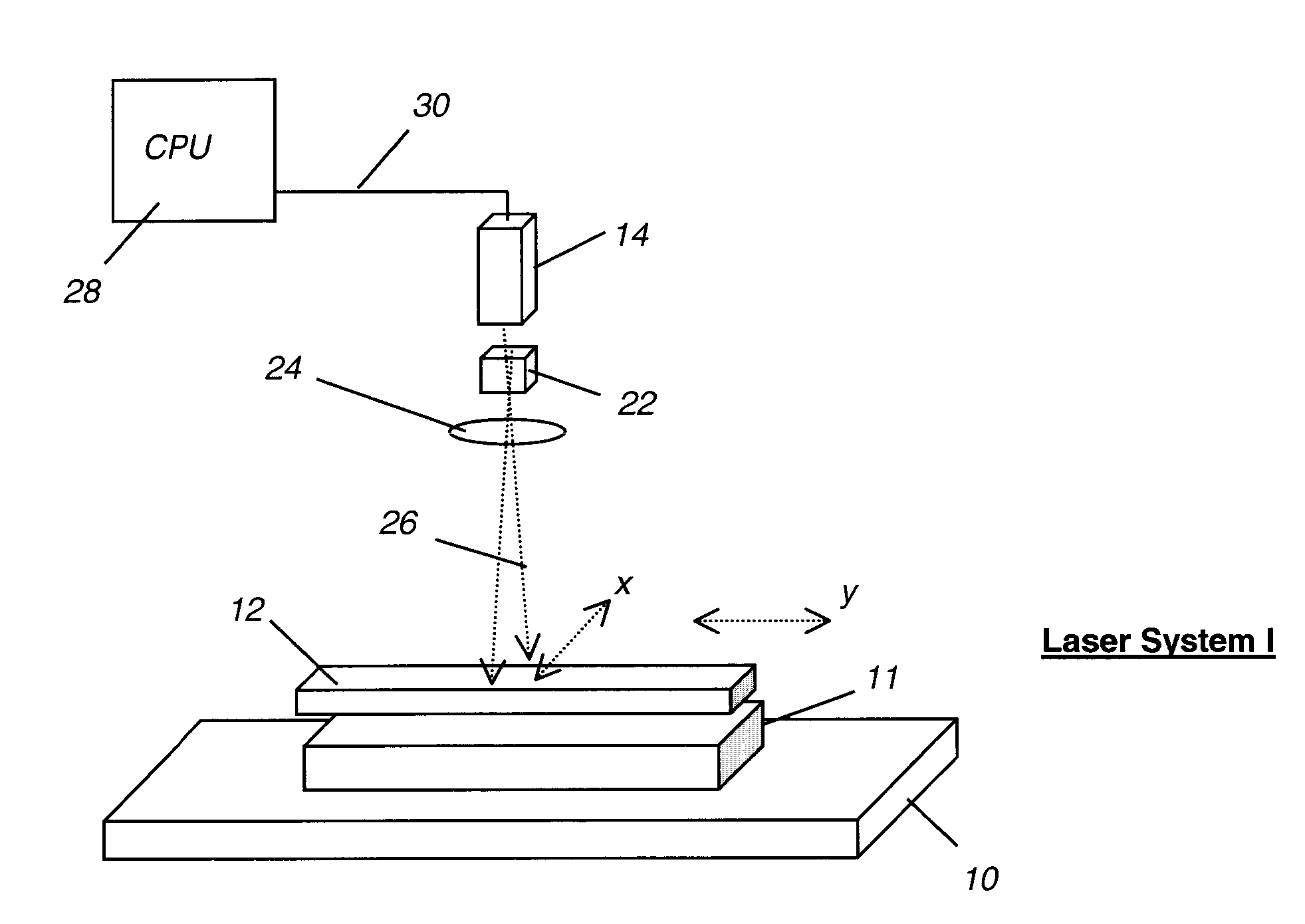
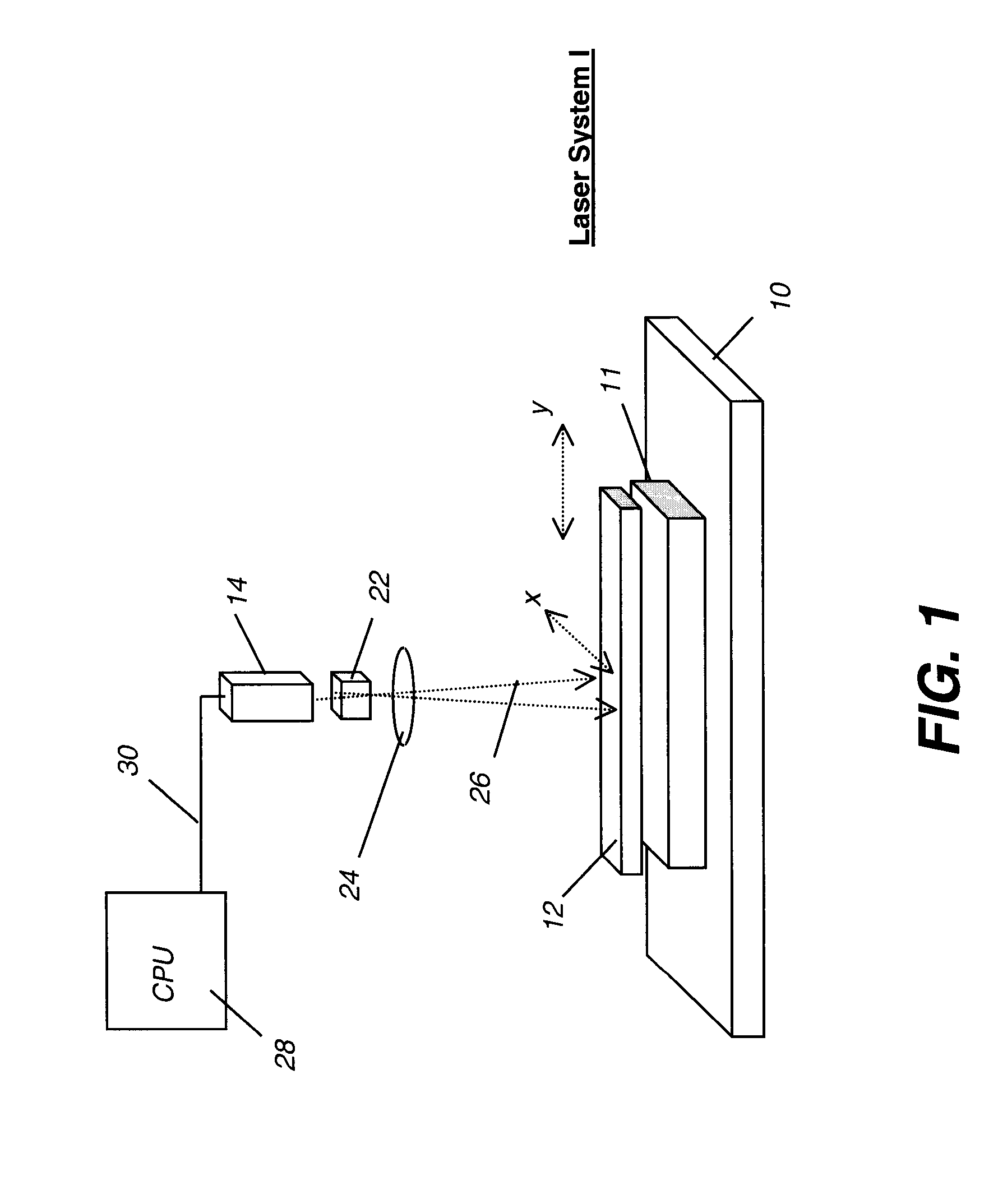
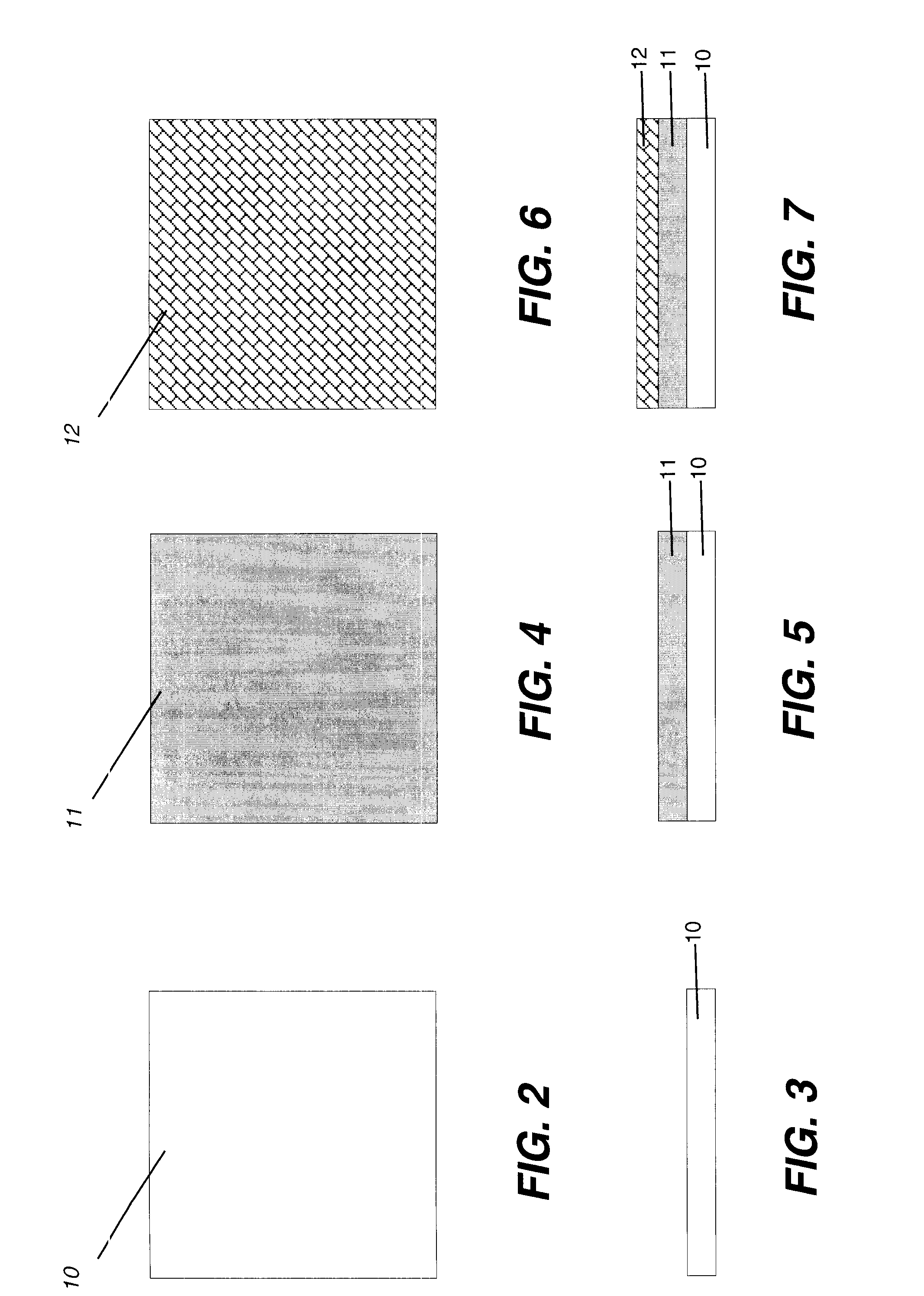
[0079]On a 1.1 mm glass substrate with between 500 and 1000 Angstroms of sputtered aluminum, a laser ablative resist layer was applied by spin coating a solution of 5 wt % Poly(methyl-co-ethyl)cyanoacrylate, 1.0 wt % IR dye (1), 0.5 wt % Cyan Dye (1), 0.05% Fluorcarbon surfactant FC-431 (3M Corp) in 50 / 50 Acetonitrile / Cyclopentaone at 1000 RPM resulting in a dry thickness of about 0.33 microns.
[0080]Portions of the ablative resist layer were removed in a pattern of intelligence by Laser System I consisting of a single infrared laser beam at 830 nm. The beam size was approximately 16 micrometers by 80 micrometers to the 1 / e2 point scanning along the wide beam direction. Relative movement between the laser beam and the resist and aluminum coated substrate was provided by a galvanometer that included a moveable mirror that scans the beam through an f-theta lens to form a scan line in wide beam direction. The dwell time was 0.9 milliseconds [Scan frequency was 10 Hz with a power setting...
example ii
[0082]On a 1.1 mm glass substrate with about 1000 Angstroms of sputtered aluminum, a laser ablative resist layer was applied by spin coating a solution of 7.5 wt % Poly(methyl-co-ethyl)cyanoacrylate, 1.0 wt % IR dye (1), 0.5 wt % Cyan Dye (1), 0.05% Fluorcarbon surfactant FC-431 (3M Corp) in 50 / 50 Acetonitrile / Cyclopentaone at 4000 RPM resulting in a dry thickness of about 0.33 microns.
[0083]Portions of the ablative resist layer were removed in a pattern of intelligence by Laser System II consisting of a non-coherent infrared diode laser beam at 808 nm whose beam is divided into 256 separate addressable channels modulated by a spatial light modulator at 5 micron intervals across the beam's width. The beam was scanned across the sample by a movable stage that held the sample at speeds between 1.0 and 0.1 meter per second. For the purpose of this example, 32 of the 256 available channels were activated. Power densities used were between 11 and 38 milliwatts per channel. Removal of the...
example iii
[0086]A glass substrate was coated in ascending order, with 50 nm Chromium, 300 nm Silicon Nitride, 200 nm amorphous silicon, and 50 nm n-doped amorphous silicon by the PECVD process. To this substrate, a laser ablative resist layer was applied by spin coating a solution of 10 wt % Poly(methyl-co-ethyl)cyanoacrylate, 1.0 wt % IR dye (1), 0.5 wt % Cyan Dye (1), 0.05% Fluorcarbon surfactant FC-431 (3M Corp) in 50 / 50 Acetonitrile / Cyclopentanone at 1000 RPM resulting in a dry thickness of about 1.0 microns.
[0087]Portions of the ablative resist layer were removed in a pattern of intelligence by Laser System II consisting of a grid of 10 micron ablated lines in the both the vertical and horizontal directions separated by 100 microns. After oxygen plasma treatment as described in Example II to remove any residual resist in the ablated regions, the substrate was treated with an SF6 plasma for 2.5 min to remove the silicon and silicon nitride layers from the ablated regions. The remaining re...
PUM
 Abstract
Description
Claims
Application Information
 - R&D Engineer
- R&D Manager
- IP Professional
- Industry Leading Data Capabilities
- Powerful AI technology
- Patent DNA Extraction
Browse by: Latest US Patents, China's latest patents, Technical Efficacy Thesaurus, Application Domain, Technology Topic, Popular Technical Reports.
© 2024 PatSnap. All rights reserved.Legal|Privacy policy|Modern Slavery Act Transparency Statement|Sitemap|About US| Contact US: help@patsnap.com