Method of increasing transistor performance by dopant activation after silicidation

a technology of dopant activation and transistor, which is applied in the direction of transistors, semiconductor/solid-state device manufacturing, electric devices, etc., can solve the problems of nickel silicide formation, difficult introduction of dopant species and activation thereof, and large transistor dimensions, so as to improve the degree of dopant activation, reduce process complexity, and enhance transistor characteristics

Inactive Publication Date: 2007-12-06
GLOBALFOUNDRIES INC
View PDF5 Cites 23 Cited by
  • Summary
  • Abstract
  • Description
  • Claims
  • Application Information

AI Technical Summary

Benefits of technology

[0012]Generally, the present invention is directed to a technique that provides enhanced transistor characteristics and may have the potential for reducing process complexity by performing a high temperature anneal process, which may result in an increased degree of dopant activation, after a silicidation process. In some illustrative embodiments, the anneal process is performed as a short irradiation process, wherein heating the respective transistor areas is restricted to a short time interval of approximately 0.1 seconds and significantly less, thereby maintaining unwanted dopant diffusion during the additional activation process at a low level. Moreover, the late anneal process may provide significant advantages in the silicide processing, since the respective transistor areas may remain in a substantially amorphous state, which may lead to increased process uniformity during the silicide formation. Consequently, the advantages obtained by a short dopant activation with reduced diffusion activity may be combined with the silicide processing to enhance the uniformity thereof and / or reduce process complexity.

Problems solved by technology

The reduction of the transistor dimensions, however, creates a plurality of issues associated therewith that have to be addressed so as to not unduly offset the advantages obtained by steadily decreasing the channel length of MOS transistors.
There are challenging issues to be dealt with for the development of enhanced photolithography and etch strategies to reliably and reproducibly create circuit elements of critical dimensions, such as the gate electrode of the transistors, for a new device generation having reduced features sizes.
In particular, when extremely shallow PN junctions with high dopant concentrations are required, the introduction of the dopant species as well as the activation thereof are challenging tasks.
However, nickel silicide tends to form so-called “piping” defects, that is, silicide “stingers,” which may extend into the channel region, thereby possibly not allowing the nickel silicide to be located near the channel region as closely as desired without unduly affecting the transistor behavior.
It is believed that some of the difficulties in forming metal silicide regions arise from the diffusion behavior of the metal in the polycrystalline or crystalline silicon in the drain and source regions and the gate electrode.

Method used


Image

  • Method of increasing transistor performance by dopant activation after silicidation
  • Method of increasing transistor performance by dopant activation after silicidation
  • Method of increasing transistor performance by dopant activation after silicidation

Examples


Embodiment Construction

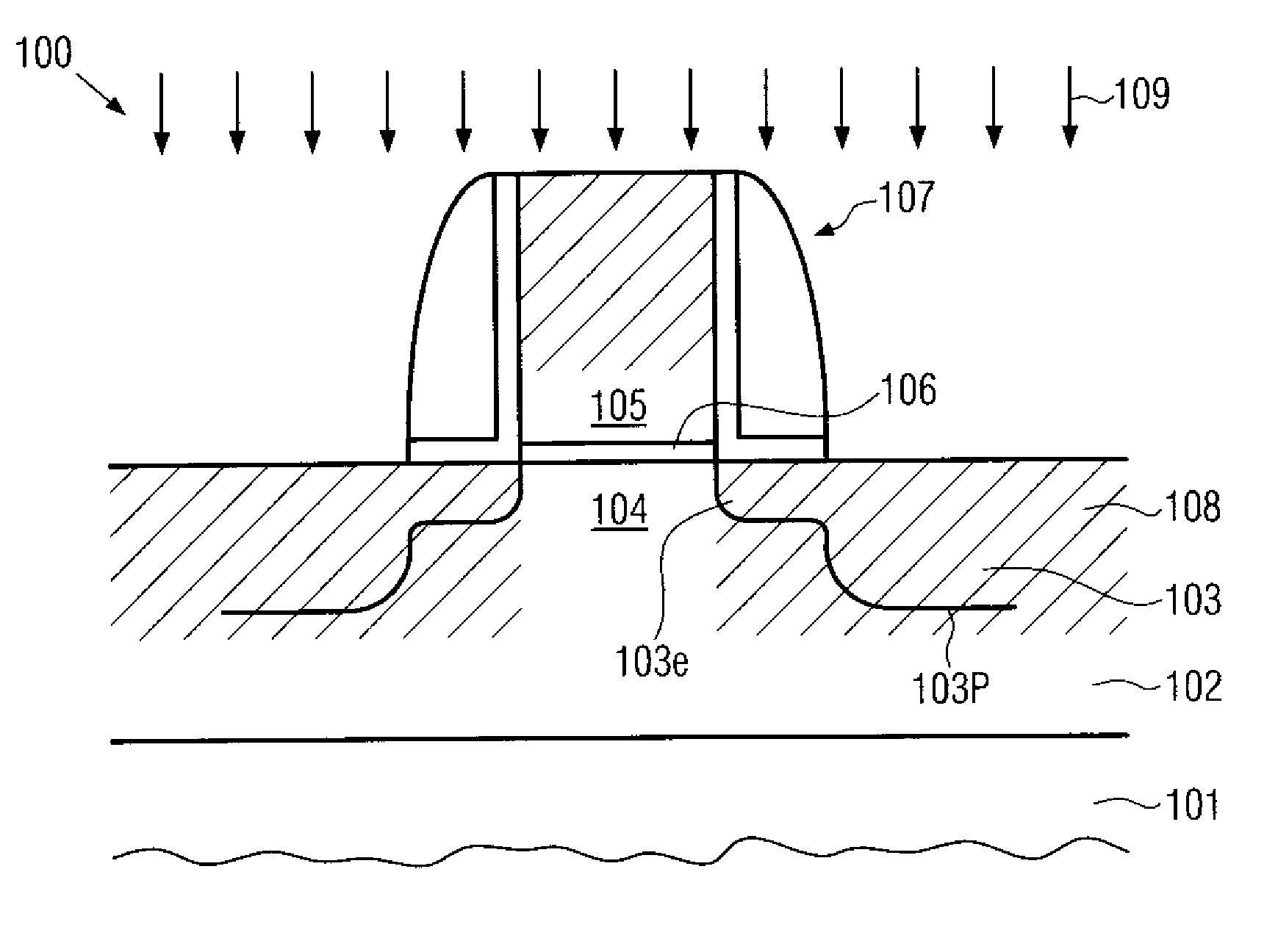
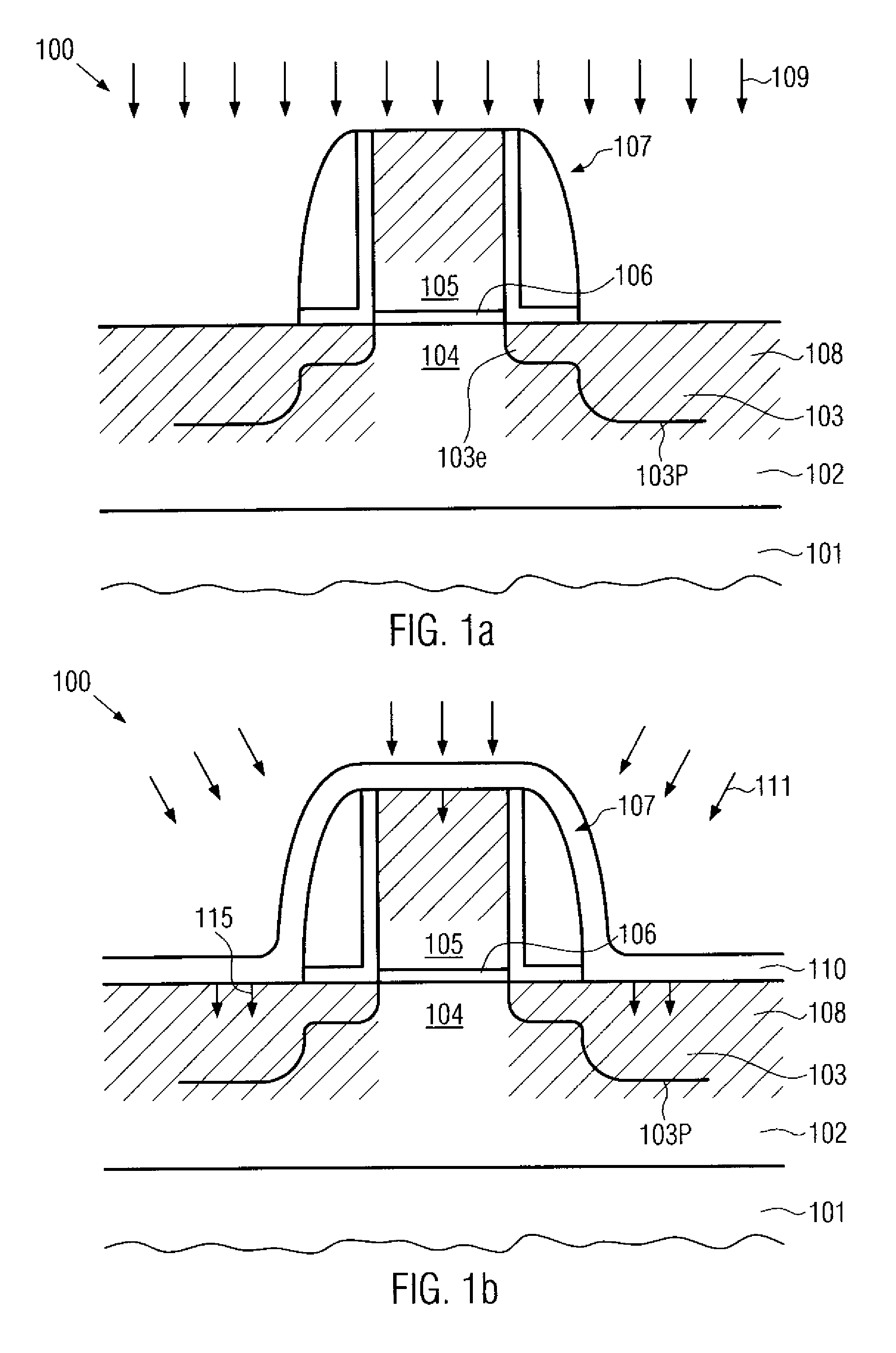
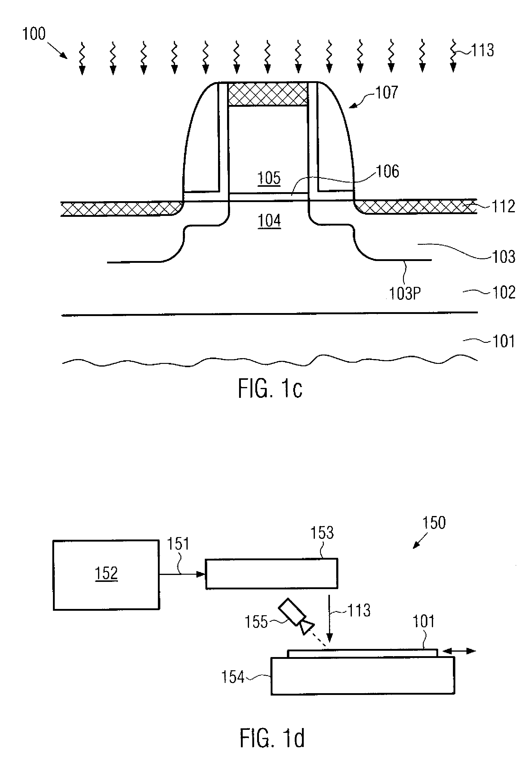
[0020]Various illustrative embodiments are described below. In the interest of clarity, not all features of an actual implementation are described in this specification. It will of course be appreciated that in the development of any such actual embodiment, numerous implementation-specific decisions must be made to achieve the developers' specific goals, such as compliance with system-related and business-related constraints, which will vary from one implementation to another. Moreover, it will be appreciated that such a development effort might be complex and time-consuming, but would nevertheless be a routine undertaking for those of ordinary skill in the art having the benefit of this disclosure.

[0021]The present subject matter will now be described with reference to the attached figures. Various structures, systems and devices are schematically depicted in the drawings for purposes of explanation only and so as to not obscure the present invention with details that are well know...


PUM

PropertyMeasurementUnit
temperatureaaaaaaaaaa
temperaturesaaaaaaaaaa
lengthaaaaaaaaaa

Abstract

By performing a laser-based or flash-based anneal process after silicidation, the degree of dopant activation with reduced diffusion activity may be accomplished, while the characteristics of the metal silicide may be improved or the complexity for manufacturing the same may be reduced.

Description

BACKGROUND OF THE INVENTION[0001]1. Field of the Invention[0002]Generally, the present disclosure relates to the formation of integrated circuits, and, more particularly, to an integration scheme for enhancing performance characteristics of MOS transistors.[0003]2. Description of the Related Art[0004]The fabrication of integrated circuits requires the formation of a large number of circuit elements on a given chip area according to a specified circuit layout. Generally, a plurality of process technologies are currently practiced, wherein, for complex circuitry, such as microprocessors, storage chips and the like, MOS technology is currently one of the most promising approaches, due to the superior characteristics in view of operating speed and / or power consumption and / or cost efficiency. During the fabrication of complex integrated circuits using MOS technology, millions of field effect transistors, e.g., N-channel transistors and P-channel transistors, are formed on a substrate inc...

Claims


Application Information

Patent Timeline
Patent Type & Authority Applications(United States)
IPC IPC(8): H01L21/44
CPCH01L21/26513H01L21/26586H01L21/268H01L29/7843H01L29/665H01L29/6656H01L29/6659H01L21/7624
Inventor PRESS, PATRICKFEUDEL, THOMASBLOOMQUIST, JOEHORSTMANN, MANFRED
Owner GLOBALFOUNDRIES INC
Why Eureka
Try Eureka