Transparent Conductor, Transparent Electrode, Solar Cell, Light Emitting Device And Display Panel

a technology of transparent conductors and electrodes, applied in the direction of non-metal conductors, identification means, instruments, etc., can solve the problems of low indium content in earth crust, high power consumption structure, and large power consumption, so as to increase the electric conductivity, suppress the resistivity, and maintain the effect of transparency

Inactive Publication Date: 2007-12-13
KANAGAWA INST OF IND SCI & TECH
View PDF7 Cites 28 Cited by
  • Summary
  • Abstract
  • Description
  • Claims
  • Application Information

AI Technical Summary

Benefits of technology

[0040] The present invention enables a remarkable increase of the electric conductivity while maintaining the transparency by using M:TiO2 obtained by replacing Ti site of an anatase type TiO2 with another metal atom (Nb, Ta, Mo, As, Sb, W, or the like) or the like. The crystalline form of the M:TiO2 may a single crystal or a polycrystal.
[0041] Particularly, when the Nb substitution is 0.1 to 20% as the ratio of the number of Nb and Ti atoms (Nb/Ti) in the metal oxide, it becomes possible to suppress the resistivity to a level of 10−4 Ωcm.
[0042] When the Nb substitution is 1 to 20% as the ratio of the number of Nb and Ti atoms (Nb/Ti) in the metal oxide, it becomes possible to suppress the resistivity to a level of 10−4 Ωcm while the internal transmittance is maintained at a high level.
[0043] When the Nb substi

Problems solved by technology

Particularly, an organic electroluminescence (EL) device developed recently is a self-luminous type device and can be effectively applied to a small portable device, however, there are problems in which the organic EL device is a current driven device and has a large power consumption Furthermore, a plasma display panel (PDP) which is spreading in the market recently and a field emission display (FED) currently developed as a next-generation display have a problem in that they have high power consumption structures.
The ITO film has superior transparency and high conductivity, howeve

Method used


Image

  • Transparent Conductor, Transparent Electrode, Solar Cell, Light Emitting Device And Display Panel
  • Transparent Conductor, Transparent Electrode, Solar Cell, Light Emitting Device And Display Panel
  • Transparent Conductor, Transparent Electrode, Solar Cell, Light Emitting Device And Display Panel

Examples


Embodiment Construction

[0096] Embodiments of the present invention are explained in detail with reference to drawings.

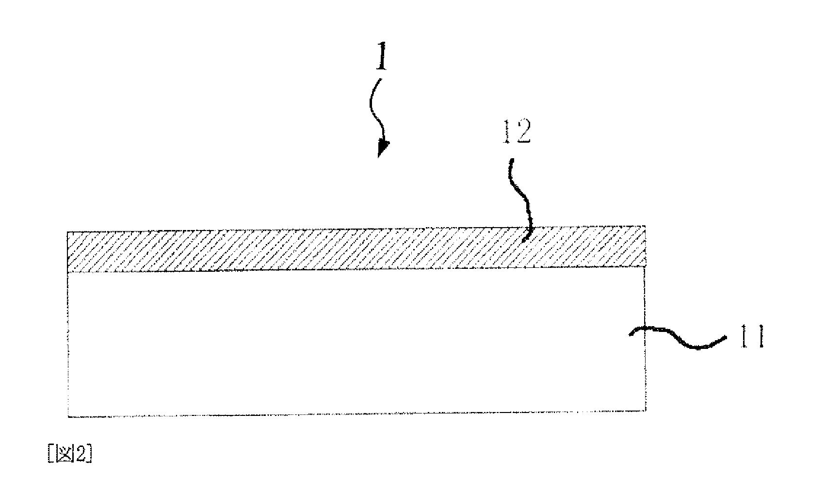
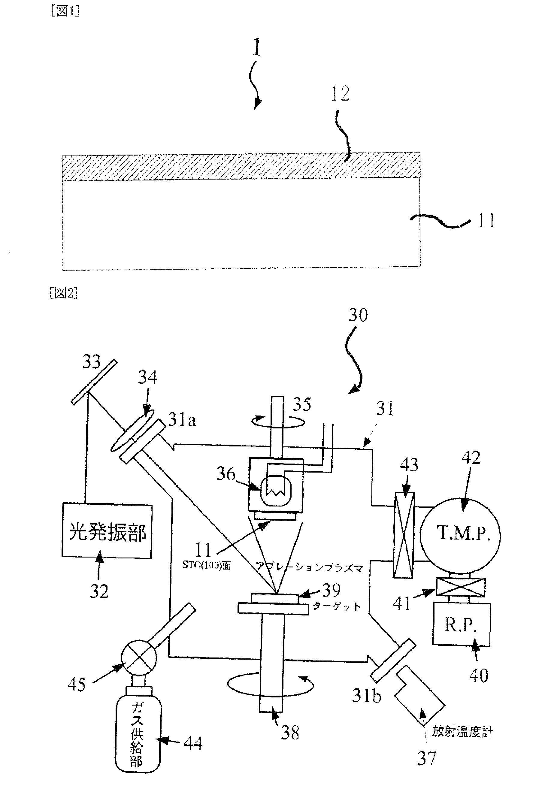
[0097] The present invention is applied for use as a transparent metal (transparent conductor) 1 to be applied to electrodes of display panels, organic ELs, solar cells, or the like. The present invention comprises a metal oxide layer 12 formed on a substrate 11 as a polycrystal or single crystal as shown in FIG. 1.

[0098] The transparent metal 1 shows metallic electric conductivity in the transparent conductor until the cryogenic temperature (5K) in which the metallic electric conductivity is defined to have 10−2 Ωcm or less of resistivity at room temperature and dR / dT>0 (R: resistivity, T: temperature) of temperature dependency of resistivity. The metallic electric conductivity preferably has 10−3 Ωcm or less resistivity at room temperature in view of increasing general use.

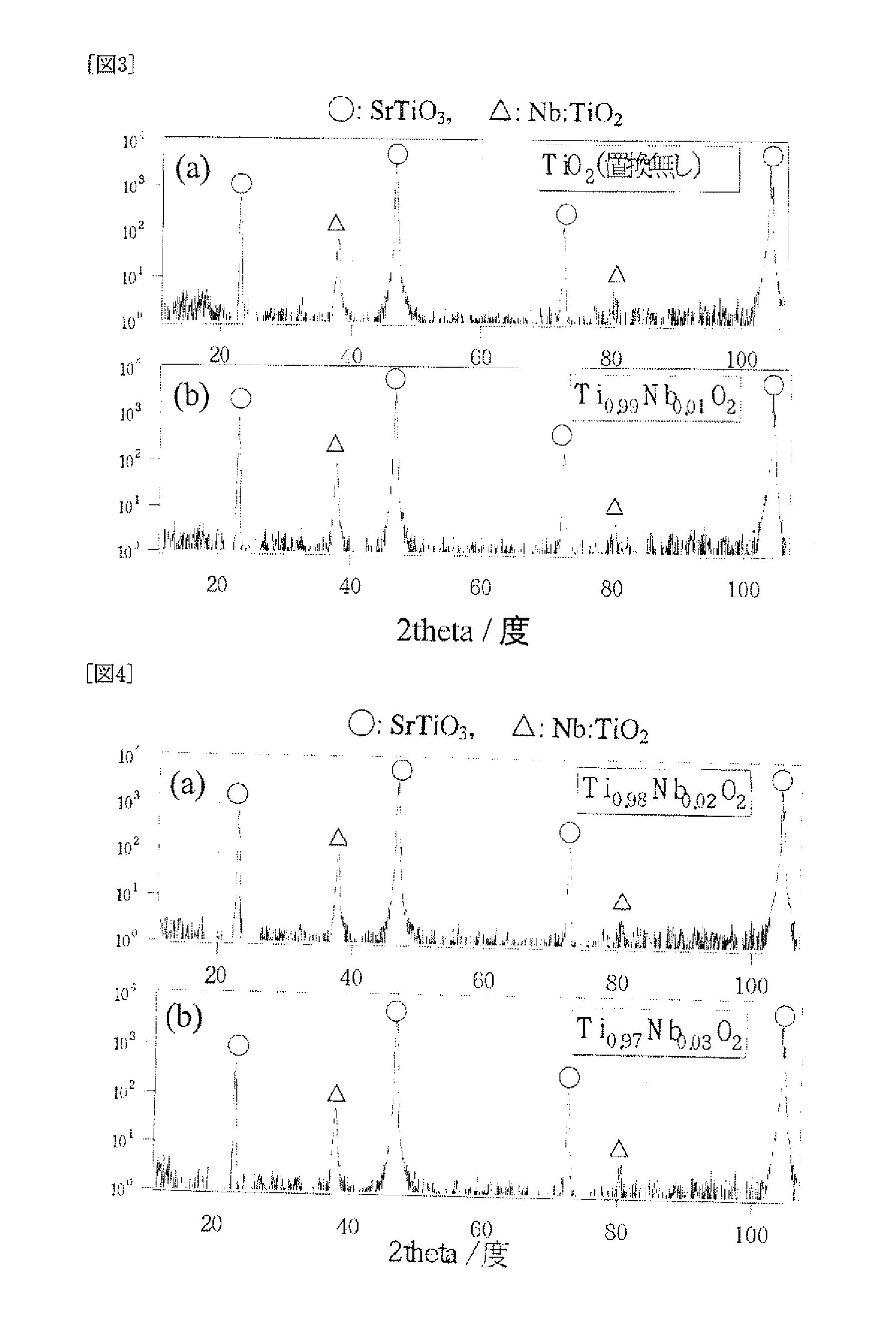
[0099] The substrate 11 is composed of strontium titanate (SrTiO3) formed so that a substrate surface 11a is a (1...


PUM

PropertyMeasurementUnit
Electrical resistivityaaaaaaaaaa

Abstract

With regard to a substrate for a transparent electrode and transparent conductive thin film each having transparency and conductivity, a transparent metal material and transparent electrode are provided which are capable of being stably supplied and are composed of raw materials with superior chemical resistance. When a metal oxide layer (12) composed of an anatase type crystal structure is provided on a substrate (11) to constitute the metal oxide layer (12) by M:TiO2, low resistivity is achieved while internal transmittance is maintained. M:TiO2 obtained by substituting other atoms (Nb, Ta, Mo, As, Sb, or W) for Ti of the anatase type TiO2 enable maintenance of transparency and remarkably improvement of electric conductivity.

Description

TECHNICAL FIELD [0001] The present invention relates to a transparent conductor to be applied for a liquid crystal panel, a solar cell, an organic electroluminescence (EL) electrode, and the like. BACKGROUND ART [0002] In recent years, needs for enlargement of liquid crystal display panels and needs for smaller-size and portability have risen. In order to achieve these, low power consumption of a display device is required and it is necessary to apply a transparent electrode having high visible light transmittance and low resistance value. [0003] Particularly, an organic electroluminescence (EL) device developed recently is a self-luminous type device and can be effectively applied to a small portable device, however, there are problems in which the organic EL device is a current driven device and has a large power consumption Furthermore, a plasma display panel (PDP) which is spreading in the market recently and a field emission display (FED) currently developed as a next-generatio...

Claims


Application Information

Patent Timeline
IPC IPC(8): H01B5/14G02F1/1343H01M14/00H05B33/28H05B33/14G09F9/30H01L33/36H01L33/42
CPCC03C17/2456Y02E10/50C03C2217/212C03C2217/218C03C2217/23C03C2217/24C03C2218/15G02F1/13439G02F2201/12G02F2202/06G02F2203/01H01B1/08H01L31/022466H01L31/1884H01M4/48H01M14/005H05B33/28Y10T428/12667C03C17/34H01L31/022475H01L31/022483Y02E60/10H01B5/14G02F1/1343
Inventor FURUBAYASHI, YUTAKAHASEGAWA, TETSUYAHITOSUGI, TARO
Owner KANAGAWA INST OF IND SCI & TECH
Why Eureka
Try Eureka