Incident light angle detector for light sensitive integrated circuit

Active Publication Date: 2007-12-20
MITUTOYO CORP
View PDF14 Cites 66 Cited by
  • Summary
  • Abstract
  • Description
  • Claims
  • Application Information

AI Technical Summary

Benefits of technology

[0008]In various embodiments, at least one material layer is formed between the first mask layer and the second mask layer, and the at least one material layer comprises at least one optically transmissive insulating layer. In a further embodiment, each material layer formed between the first and second mask layers is formed by a process step that is used to

Problems solved by technology

For at least this reason, at least one aspect of a combination of features including fabrication cost, size, and/or the measurement resolution of the disclosed detector configurations is undesirable for many a

Method used


Image

  • Incident light angle detector for light sensitive integrated circuit
  • Incident light angle detector for light sensitive integrated circuit
  • Incident light angle detector for light sensitive integrated circuit

Examples


first embodiment

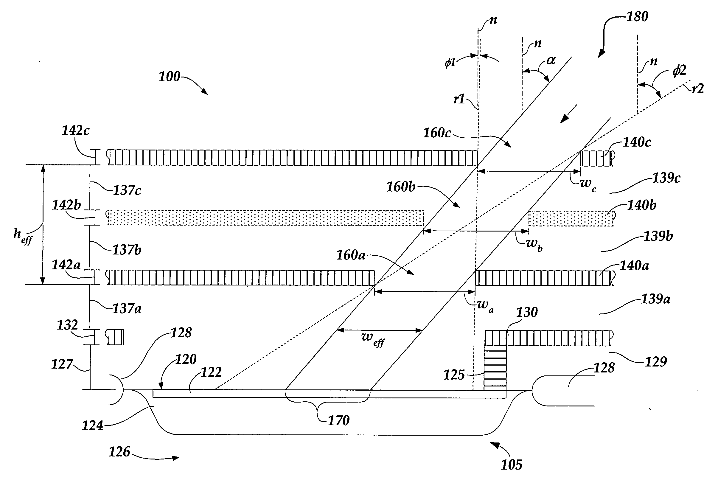
[0022]FIG. 1 is a diagram of a detector configuration 100 with an angled interlayer optical path 180 directed toward a photodetector 105 for sensing radiation at an angle of incidence corresponding to an angle α. The detector configuration 100 may be one of a plurality of similar configurations included a photodetector IC. The function of the detector configuration 100 may be an auxiliary function of the photodetector IC (e.g., an imaging array IC) as described in greater detail below. Each reference line n shown in FIG. 1 represents a vector normal to a nominal surface plane of the photodetector IC. While a photodiode type photodetector is illustrated, it will be appreciated that any light sensitive element could also be utilized, such as a photogate, photo-transister, etc. The term light, as used herein, is not restricted to visible radiation. As shown in FIG. 1, the photodetector 105 includes a surface 120, an N+ diffusion layer 122, a P well 124, a P substrate 126 and a field ox...

second embodiment

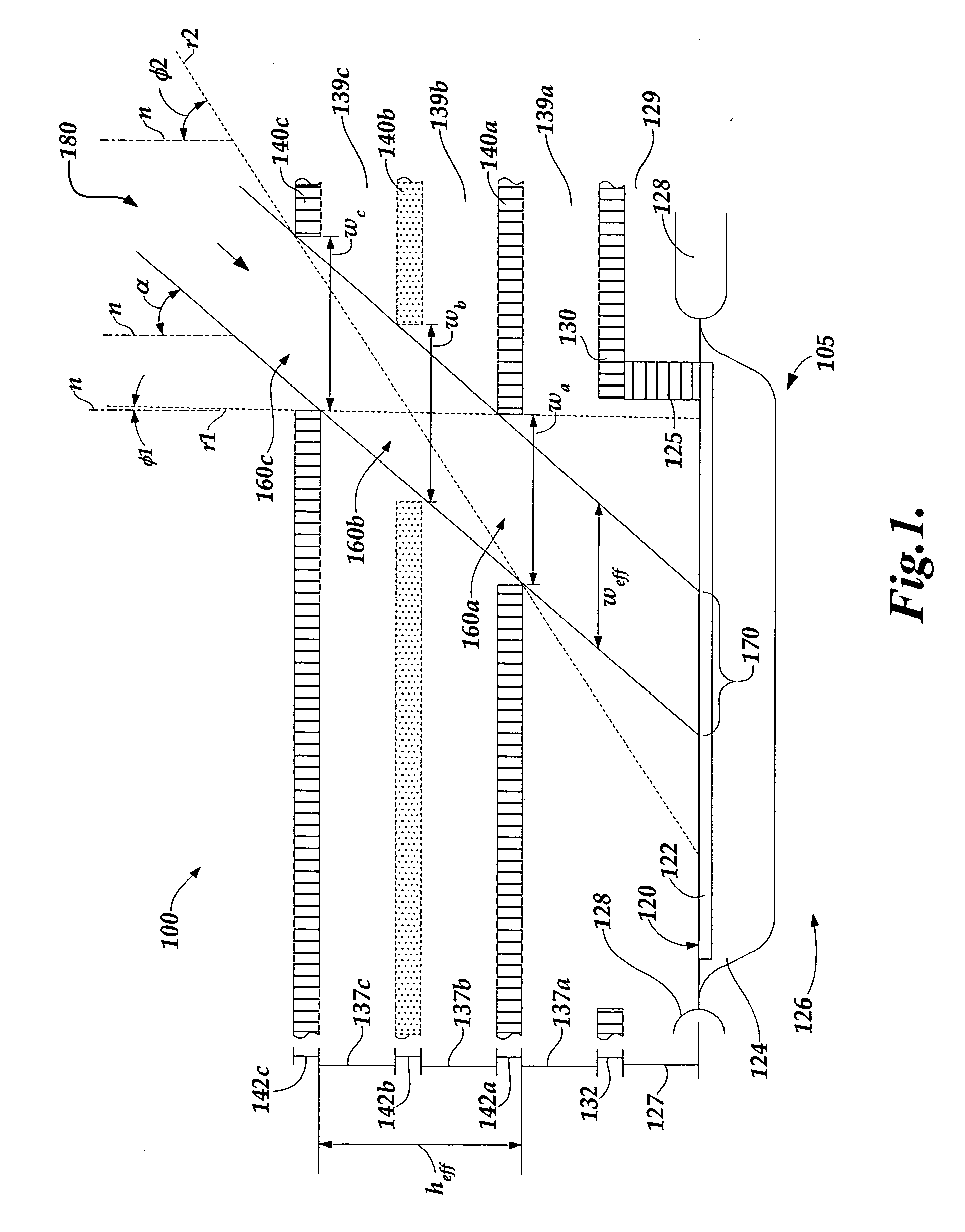
[0030]FIG. 2 is a diagram of a detector configuration 200 with an angled interlayer optical path 180′ directed toward a photodetector 105 for sensing radiation at an angle of incidence corresponding to an angle α. The illustrated components of the detector configuration 200 are similar to those of FIG. 1, except as otherwise described below. Each of the metal layers 130, 140a, 140b′ and 140c and insulating layers 129, 139a, 139b, 139c, may be similarly fabricated and have similar thicknesses.

[0031]In contrast to the detector configuration 100, in the embodiment shown in FIG. 2, the “interior” metal layer 140b′ provides an important function in defining the angled interlayer optical path 180′, and is not optional in the vicinity of the photodetector 105. It should be appreciated that when the thicknesses and materials of each metal layer and each insulating layer are advantageously the standard thicknesses and materials used to fabricate other structures on the photodetector IC, that...


PUM


Abstract

A detector configuration determines the direction of illumination incident on a photosensitive device. Multiple mask layers include holes which form an interlayer optical path through which radiation reaches a photodetector. The interlayer optical path provides a selected nominal maximum signal angle and the detector senses when radiation is received at or near that angle. In one embodiment, three holes in three metallization layers provide an arbitrarily narrow interlayer optical path with improved angular detection relative to that provided by two holes. An illumination direction-sensing array may use multiple instances of the detector configuration. The detector configuration may provide enhanced utility and economy by being adapted to use only those fabrication steps used for fabricating other primary circuits on an IC.

Description

FIELD OF THE INVENTION[0001]The invention relates generally to a detector configuration for determining an angle of incidence of light on a photodetector, and in one example embodiment, the detector configuration may be utilized to indicate the degree of photodetector and / or light source misalignment in position encoders or the like.BACKGROUND OF THE INVENTION[0002]Various angle of incidence detectors are known, such as those disclosed in U.S. Pat. No. 4,857,721 to Dunavan, et al., European Patent Specification EP 0747719 to Cantin, et al., and U.S. Patent Application Publication No. 2002 / 0053635 to Schroter, et al., each of which is incorporated herein by reference. However, each of the preceding references teaches that at least one “shadow mask” critical to the operation of the disclosed devices is formed separately from the photodetector elements of the disclosed devices. For at least this reason, at least one aspect of a combination of features including fabrication cost, size, ...

Claims


Application Information

Patent Timeline
IPC IPC(8): H01L31/0232
CPCH01L27/1446H01L27/14603H01L31/02024H01L31/02164H01L27/14623H01L27/14605
Inventor SHAFFER, JAMIE LYN
Owner MITUTOYO CORP
Why Eureka
Try Eureka