[0005] The object of the present invention is to provide a control circuit and a control method, which render possible improved switching performance of an electronic circuit.
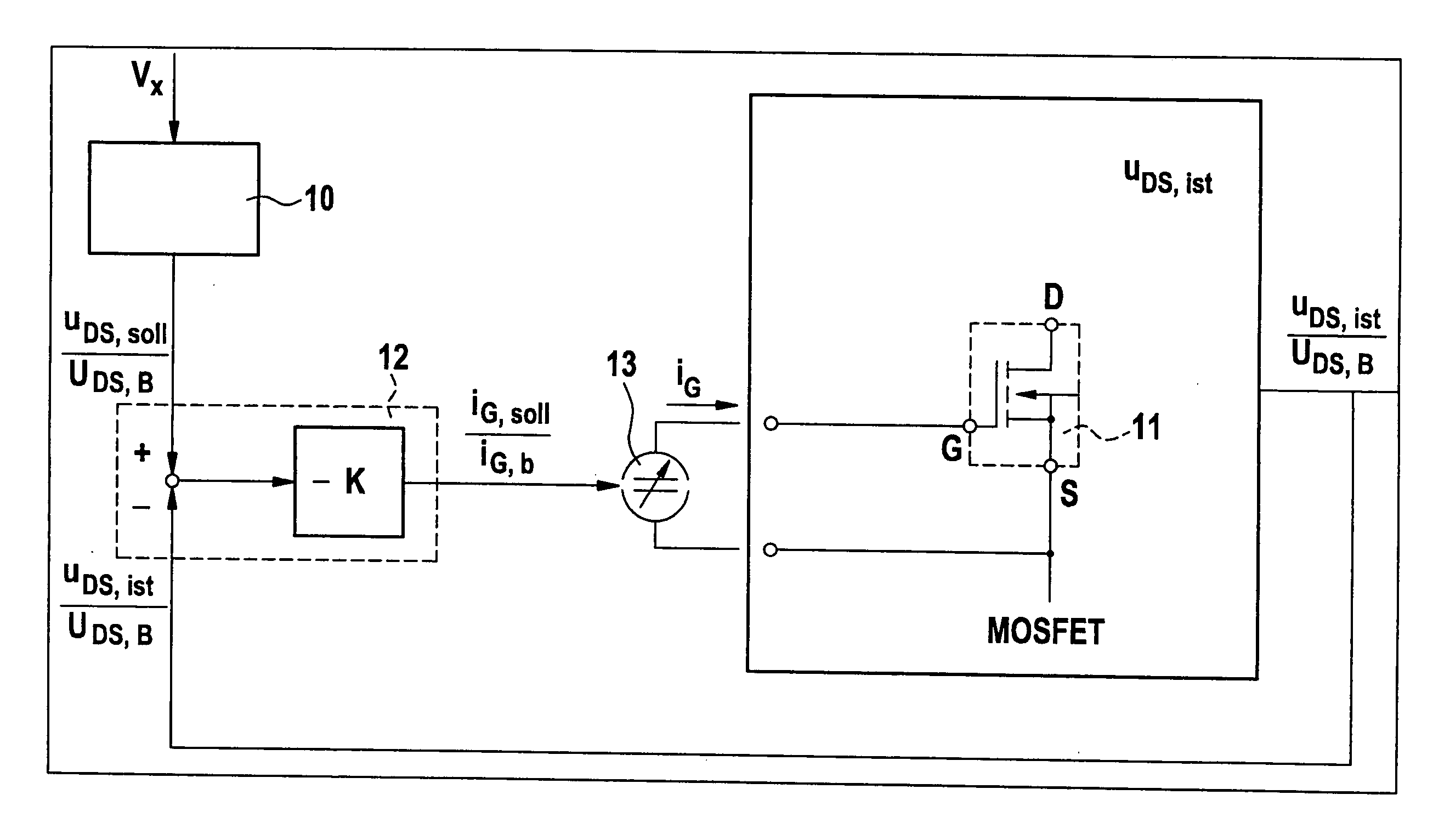
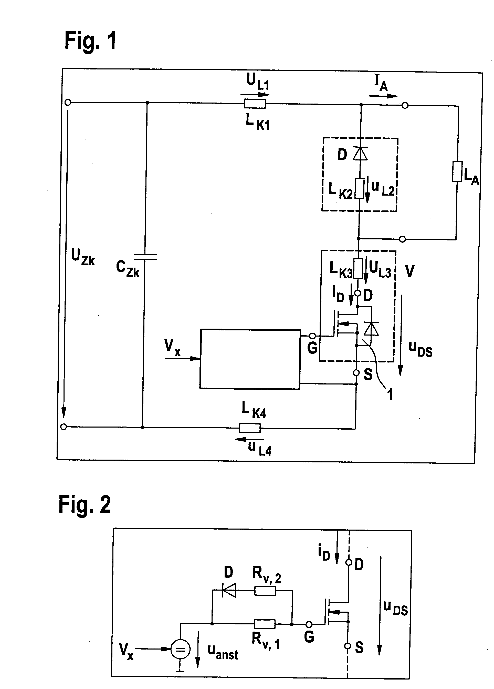
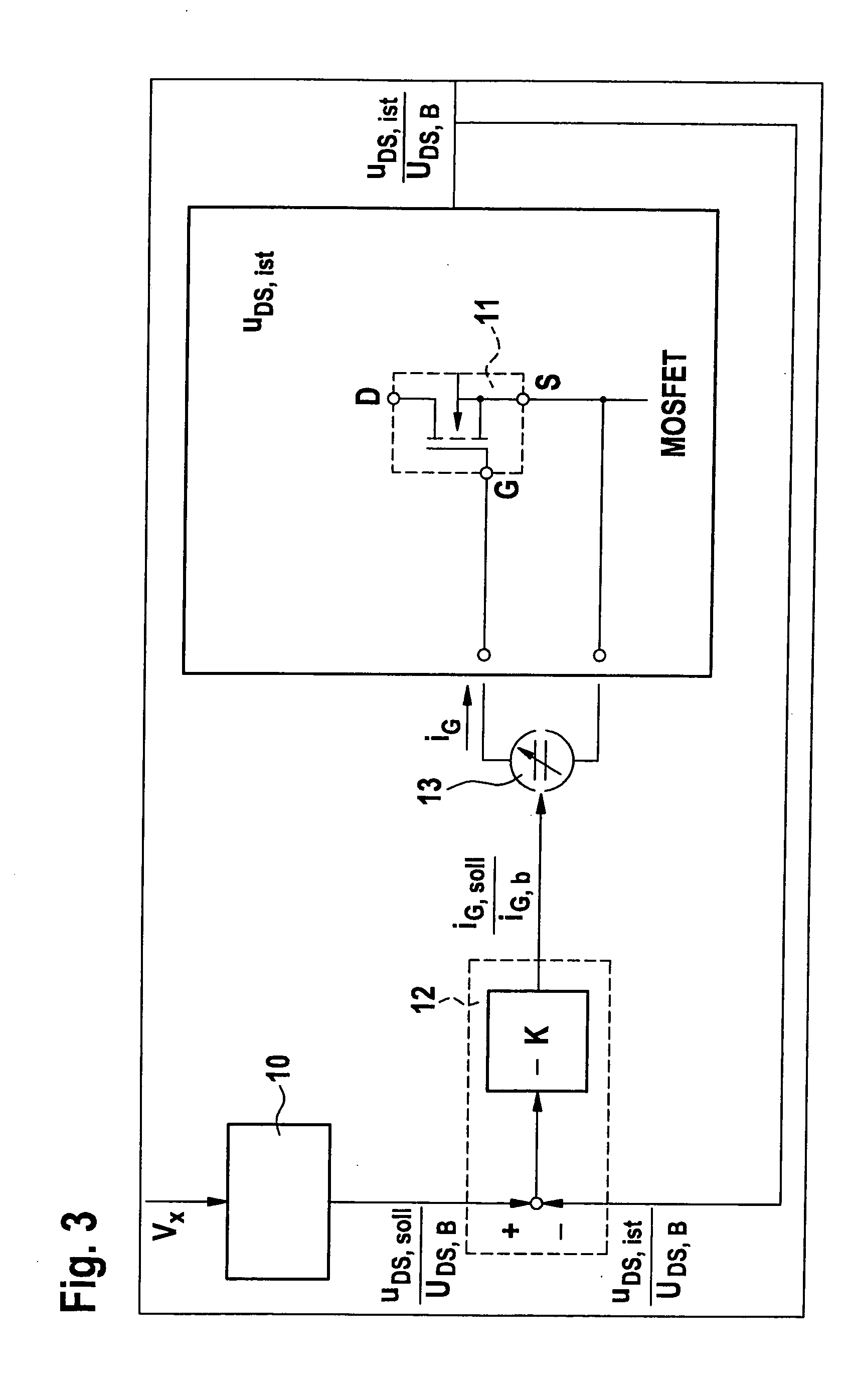
[0007] The idea of the present invention is to reduce and control the high excess voltages between the terminals of a semiconductor switch during the circuit-closing and circuit-breaking operations, the excess voltages being formed due to inductances in the current path to be switched. This is achieved by applying a controlled control
voltage to the control terminal of the semiconductor switch, the control
voltage being set as a function of the
terminal voltage at the semiconductor switch. Since the semiconductor switch can normally only tolerate a maximum voltage between the current-carrying terminals, a
setpoint terminal voltage is defined, the control voltage being controlled in such a manner, that the
setpoint terminal voltage is not exceeded. This allows the commutation voltage to be directly specified, which means that on one hand, the
dielectric strength of the utilized semiconductor switch may be utilized in an optimal manner and, on the other hand, the oscillations occurring during operation in response to the control according to the related art may be considerably reduced. During the control operation, the control keeps the semiconductor switch in its active operating range.
[0008] The control circuit of the present invention allows the excess voltages occurring between the current-carrying terminals of the semiconductor switch to be reduced and controlled without an additional protective circuit, and simultaneously keeps the increase in the switching losses as low as possible. The reduced excess voltage allows the disruptive electromagnetic emissions from the switching operation to be reduced, since the induced oscillation has a smaller starting amplitude and therefore decays more rapidly. This allows the filter and shielding measures to be designed to be less complicated and, therefore, more cost-effective.
[0009] In the case of power field-effect transistors, closing resistance RDS,on increases superproportionally to the maximum blocking voltage, but is inversely proportional to the
chip area of the field-effect
transistor. Limiting the excess voltage allows field-effect transistors having a lower
breakdown voltage to be used. These have a lower closing resistance with the same
chip area, which means that the efficiency of the
power electronics may be increased. On the other hand, if field-effect transistors having a smaller
chip area and the same closing resistance RDS,on as a larger field-effect transistor are used, a reduction in volume occurs.
[0015] In the case of a circuit-closing operation, the
control unit preferably adjusts the setpoint terminal voltage to a first setpoint value initially, and then adjusts it to a second setpoint value after a period of time elapses, the second setpoint value being less than or equal to a low operating potential in the case of a self-blocking semiconductor switch, or greater than or equal to a high operating potential in the case of a self-conducting semiconductor switch. Such a two-stage switching operation is useful for being able to control the excess voltages during the circuit-closing operation in the most effective manner possible. To this end, in accordance with the first setpoint value, the semiconductor switch is preferably operated in its active operating range during the period of time. In order to limit the forward power losses in the semiconductor switch, the second setpoint value must be set as the setpoint terminal voltage after expiration of the period of time, in order to completely switch the semiconductor switch through, so that the semiconductor switch is not destroyed by the high forward power losses. If the second setpoint value were to be properly specified at the start of the circuit-closing operation, i.e. if the circuit-closing operation is only performed by specifying a setpoint terminal voltage, which is less than or equal to a low operating potential or greater than or equal to a high operating potential as a function of the
conductivity type of the utilized semiconductor switch, the control unit would attempt to completely switch the semiconductor switch on as rapidly as possible. This would result in the commutation voltage at the inductors and, therefore, the rate of change of the current in the current path as well, becoming very large, which means that the switching operation would nearly correspond to a switching operation according to the related art and the voltage between the current-carrying terminals would sharply increase. The two-stage control operation allows the rate of change of the current in the current path to be reduced, so that disruptive emissions are reduced.
[0022] According to a further aspect of the present invention, a method for controlling an electronic circuit is provided. The electronic circuit has a current path through a charge-controlled semiconductor switch and a line; when the semiconductor switch is switched, the
inductance of the line and / or of the electrical components connected in the current path leads to an excess voltage between a first and a second current-carrying terminal of the semiconductor switch. A charge-controlled gate of the semiconductor switch is charged or discharged by a control current, the control current being controlled in such a manner that, in the case of a switching operation, the terminal voltage of the semiconductor switch does not exceed a predefined setpoint terminal voltage.


