

Laminate body, and method for manufacturing thin substrate using the laminate body
a technology of laminate body and thin substrate, which is applied in the direction of manufacturing tools, photomechanical equipment, instruments, etc., can solve the problems that the method cannot be practically used as a method of thinning a semiconductor wafer, and the wafer thickness has not yet reached a remarkable improvement, so as to prevent bubbles and dust contamination, the effect of reducing pressur
- Summary
- Abstract
- Description
- Claims
- Application Information
AI Technical Summary
Benefits of technology
Problems solved by technology
Method used
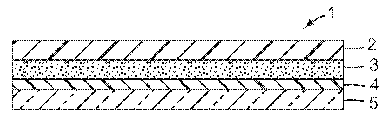
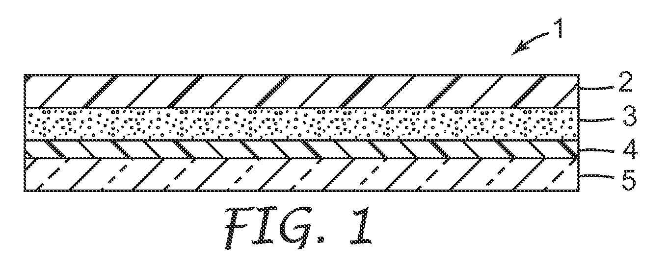
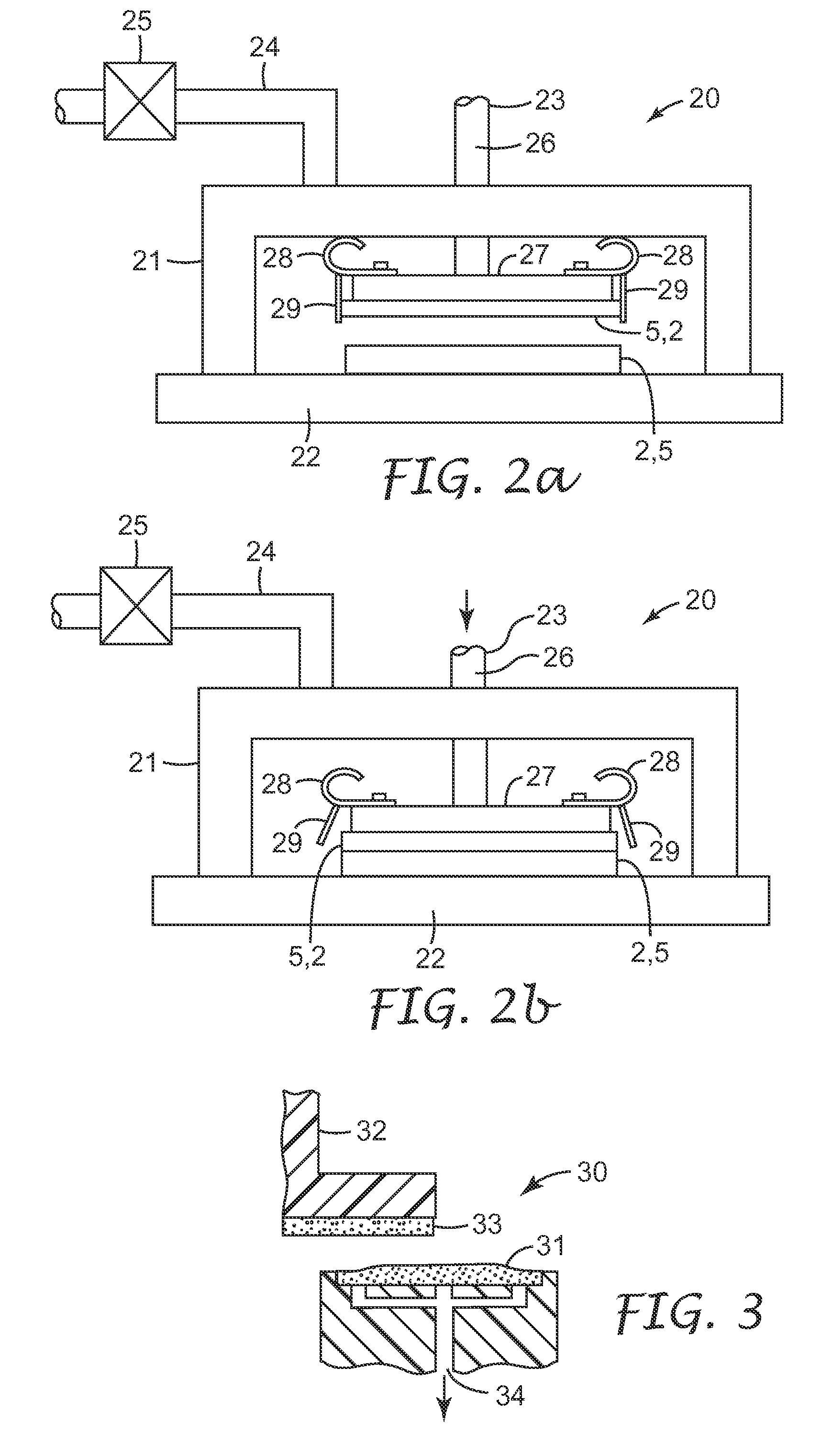
Image

Examples
example 1
[0087]A mixture of 100.0 grams of VQM-135, 7.2 grams of SYL-Off 7678, and 4.4 milligrams of Catalyst was prepared in an amber bottle. Using a notch bar coater, a 75 micrometer thick layer of this adhesive composition was coated onto the polyimide passivation layer of a silicon wafer. A piece of LTHC glass was placed on the adhesive with the LTHC layer facing the wafer. This sandwich was passed under a UV processor (Fusion D bulb, low power, exposure time approximately 15 seconds). The UV illumination passed through the glass and cured the adhesive. Upon prying the glass off of the wafer, the adhesive layer remained adhered to the glass and removed cleanly from the polyimide surface.
example 2
[0088]A mixture of 56.0 grams of VQM-135, 42.0 grams of DMS-V31 and 140.0 grams of VQX-221 was prepared in a glass bottle. The xylenes solvent was removed using a rotary evaporator attached to a vacuum pump. To the resulting mixture was added 17.5 grams of SYL-Off 7678, and 7.7 milligrams of Catalyst. Using a notch bar coater, a 75-micrometer thick layer of this adhesive composition was coated onto the polyimide passivation layer of a silicon wafer. A piece of LTHC glass was placed on the adhesive with the LTHC layer facing the wafer. This sandwich was passed under a UV processor (Fusion D bulb, low power, exposure time approximately 15 seconds). The UV illumination passed through the glass and cured the adhesive. Upon prying the glass off of the wafer, the adhesive layer remained adhered to the glass and removed cleanly from the polyimide surface.
PUM
| Property | Measurement | Unit |
|---|---|---|
| thickness | aaaaa | aaaaa |
| thickness | aaaaa | aaaaa |
| temperatures | aaaaa | aaaaa |
Abstract
Description
Claims
Application Information