Superconducting filter device and method of producing the same

a filter device and superconducting technology, applied in the direction of superconductor devices, basic electric elements, electrical apparatus, etc., can solve the problems of filter loss, superconducting film crystallinity decline, and the electrical surface resistance of the superconducting film does not improve as expected, so as to prevent current concentration on a resonator, reduce the maximum current density, and improve the effect of electrical surface resistan

Inactive Publication Date: 2008-01-24
FUJITSU LTD
View PDF4 Cites 10 Cited by
  • Summary
  • Abstract
  • Description
  • Claims
  • Application Information

AI Technical Summary

Benefits of technology

[0048]According to the above embodiments, it is known that a bulk superconducting material can be formed to have various diameters by melting, and such a bulk superconducting material can be machined to have a preset thickness. By applying such a bulk superconducting material to a high frequency transmitting filter, it is possible to prevent current concentration on a resonator.
[0049]Therefore, it is possible to reduce the maximum current density and improve the electrical surface resistance.

Problems solved by technology

However, when receiving a high-power RF signal, loss in the filter increases.
However, when the film thickness of the superconducting film is increased, the crystallinity of the superconducting film declines, so that the electrical surface resistance of the superconducting film does not improve as expected.
The bulk superconducting material, which has good crystallinity close to a single crystal, is applicable to not only magnets but also various other devices, and it is a hot issue how to apply the bulk superconducting material to actual devices.

Method used


Image

  • Superconducting filter device and method of producing the same
  • Superconducting filter device and method of producing the same
  • Superconducting filter device and method of producing the same

Examples


Embodiment Construction

[0059]Below, preferred embodiments of the present invention are explained with reference to the accompanying drawings.

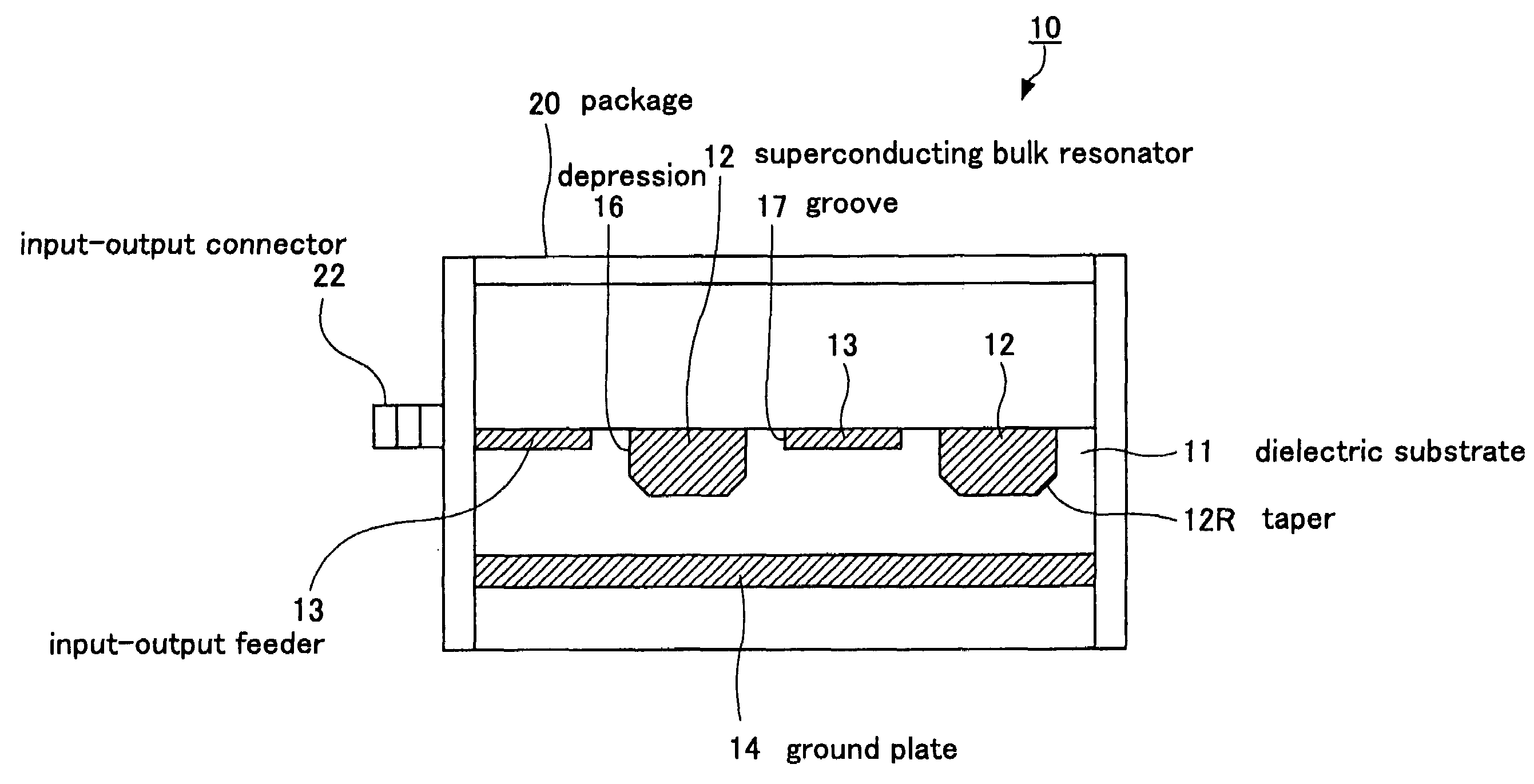
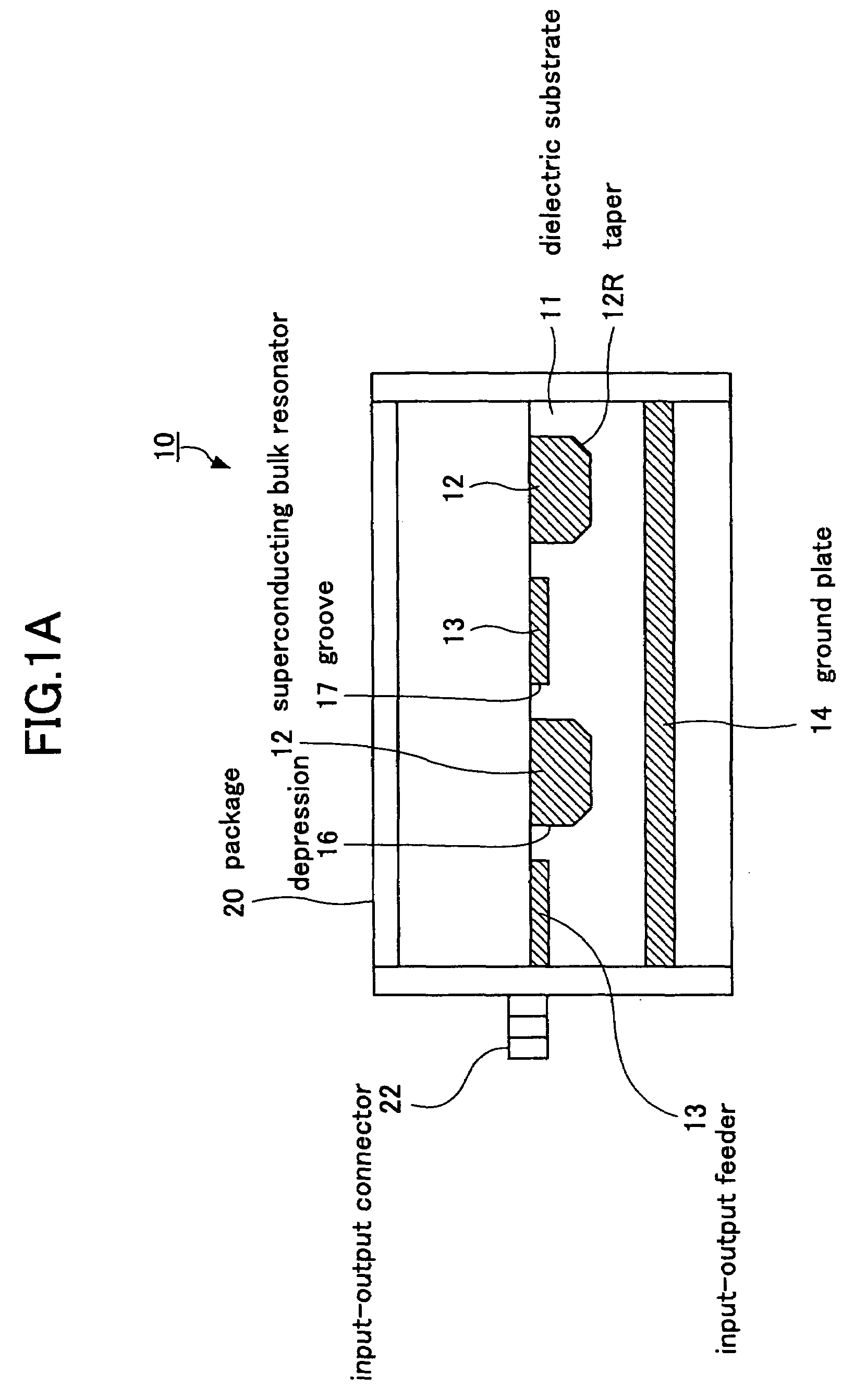
[0060]FIG. 1A and FIG. 1B are a schematic cross-sectional view and a perspective view illustrating a configuration of a superconducting filter device 10 according to an embodiment of the present invention.

[0061]For example, the superconducting filter device 10 is held in a metal package 20 and is used as a high frequency transmit filter in a base station in a mobile communication system.

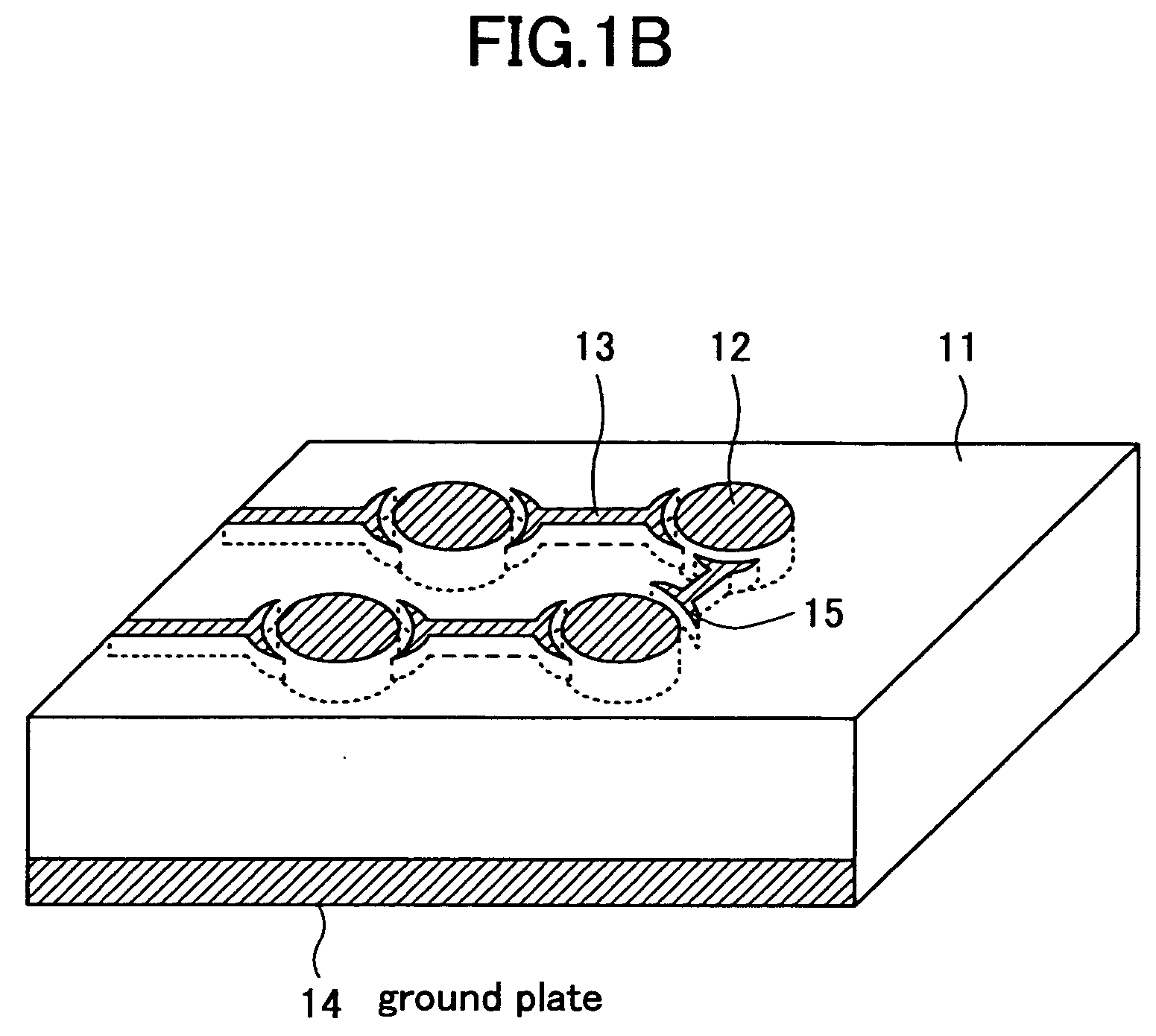
[0062]For example, the superconducting filter device 10 has a dielectric substrate 11 which is formed from a sapphire single crystal, a bulk superconducting resonator 12 which is formed from a bulk superconducting material embedded in the dielectric substrate 11, a signal input-output line (below, referred to as “feeder”) 13 arranged to extend near the bulk superconducting resonator 12, and a ground electrode (below, referred to as “ground plate”) 14 formed on the back surface of the ...


PUM

PropertyMeasurementUnit
curvature radiusaaaaaaaaaa
thicknessaaaaaaaaaa
diameteraaaaaaaaaa

Abstract

A superconducting filter device is disclosed that is able to prevent current concentration and improve electrical surface resistance. The superconducting filter device includes a first dielectric substrate, and a bulk superconducting resonator that is embedded in the first dielectric substrate and is formed from a bulk superconducting material.

Description

CROSS-REFERENCE TO RELATED APPLICATION[0001]This patent application is based on Japanese Priority Patent Application No. 2006-200792 filed on Jul. 24, 2006, the entire contents of which are hereby incorporated by reference.BACKGROUND OF THE INVENTION[0002]1. Field of the Invention[0003]The present invention relates to a superconducting filter device, particularly, to a superconducting filter device having an embedded bulk superconducting resonator, and a method of fabricating the superconducting filter device.[0004]2. Description of the Related Art[0005]In recent years and continuing, along with transition to high speed, large capacity data communications such as the next generation mobile communication system, and a wideband wireless access system, effective utilization of frequency resources becomes indispensable. A leading candidate for solving the frequency interference problem is using a high-Q superconducting filter, which has low loss and good frequency cutoff characteristics...

Claims


Application Information

Patent Timeline
Patent Type & Authority Applications(United States)
IPC IPC(8): H01P1/203H01B12/02
CPCH01P1/20381
Inventor AKASEGAWA, AKIHIKOKURIHARA, KAZUAKIYAMANAKA, KAZUNORIOHSHIMA, SHIGETOSHISAITO, ATSUSHI
Owner FUJITSU LTD
Why Eureka
Try Eureka