Tandem solar cell structures and methods of manufacturing same

a solar cell and thin film technology, applied in the field of thin film solar cell structures, can solve the problems manufacturing such complex structures, and many challenges, and achieving the effect of reducing conversion efficiency

Inactive Publication Date: 2008-01-31
SOLOPOWER
View PDF41 Cites 39 Cited by
  • Summary
  • Abstract
  • Description
  • Claims
  • Application Information

AI Technical Summary

Benefits of technology

[0018]In one aspect there is provided a polycrystalline thin film solar cell structure comprising a polycrystalline thin film absorber layer with a bottom surface and a top surface through which light enters the absorber layer; and a semi-transparent conductive layer including at least one of a ruthenium oxi...

Problems solved by technology

However, the cost of electricity generated using silicon-based solar cells is higher than the cost of electricity generated by the more traditional methods.
However, manufacturing such complex structures presents many challenges.
Otherwise, power loss due to this excess resistance would reduce the conversion efficiency.
One important challenge in manufacturing the tandem solar cell structures such as those shown in FIGS. 2 and 3 is the fabrication of the top cell with a high quality, large band-gap top cell bottom contact.
In addition to fabrication of a conductive and transparent back contact, in the case of the two terminal device of FIG. 3, there is also the challenge of processing the top cell directly onto the bottom cell.
Reactive atmospheres, high temperatures etc. needed for top cell fabrication often negatively impact the bottom cell.
The standard back contact m...

Method used


Image

  • Tandem solar cell structures and methods of manufacturing same
  • Tandem solar cell structures and methods of manufacturing same
  • Tandem solar cell structures and methods of manufacturing same

Examples


example 1

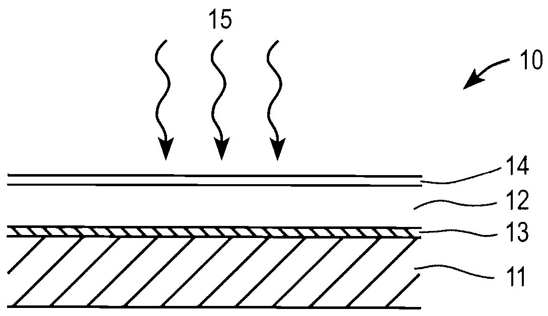
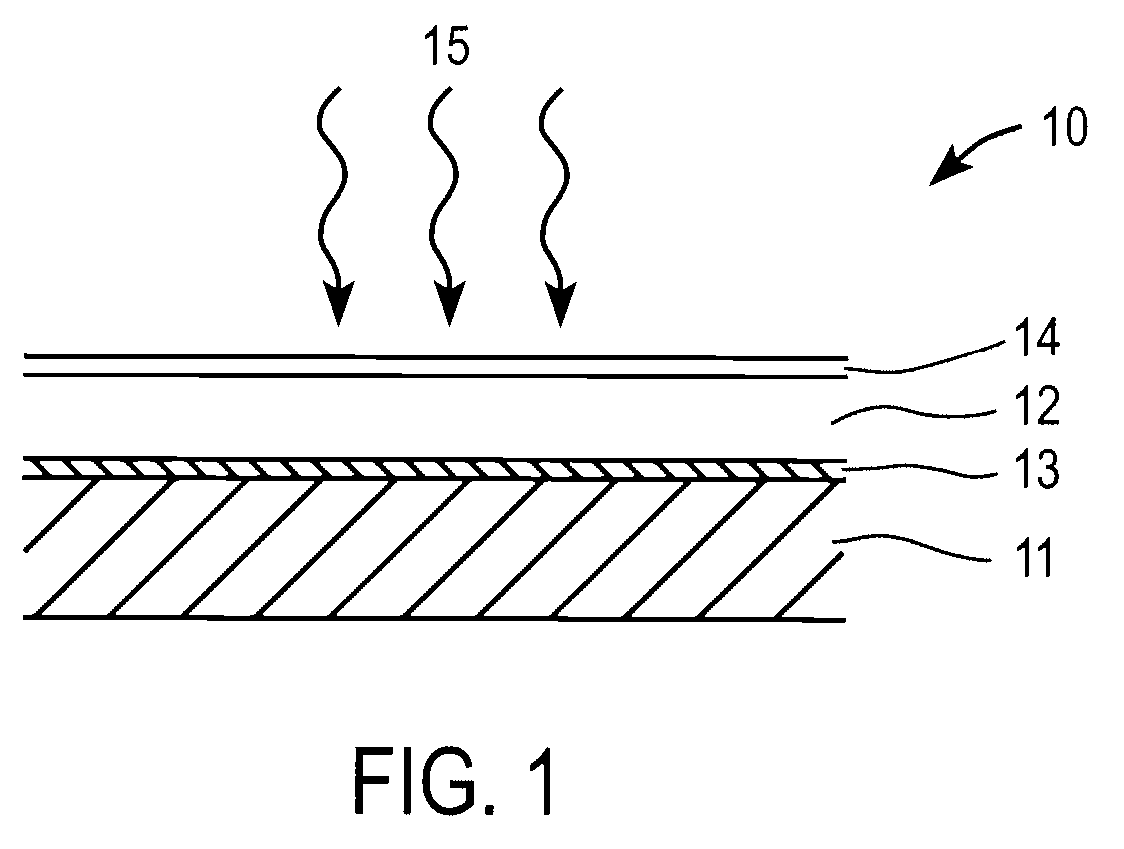
[0030]A glass sheet or transparent polymeric foil (such as polyimide) may be used as the substrate. A transparent conductive oxide (TCO) layer, such as ZO, ITO, TO etc., may then be deposited on the substrate. The thickness of the TCO layer may be in the range of 50-500 nm, the thickness being determined by the design of the device and the current carrying capacity needed. A RuO2 film may be deposited over the TCO layer. Thickness of the RuO2 film may be in the range of 2-200 nm, preferably in the range of 10-100 nm. This film may be deposited by various techniques such as evaporation, sputtering, reactive sputtering, reactive evaporation, activated reactive evaporation, oxidation of Ru films, MOCVD, electrodeposition, ink deposition etc. A thin film polycrystalline Cu(In,Ga)(S,Se)2 absorber layer may then be deposited on the RuO2 surface by various techniques well known in the field. These techniques include but are not limited to sputtering, co-evaporation, electrodeposition, ink ...

example 2

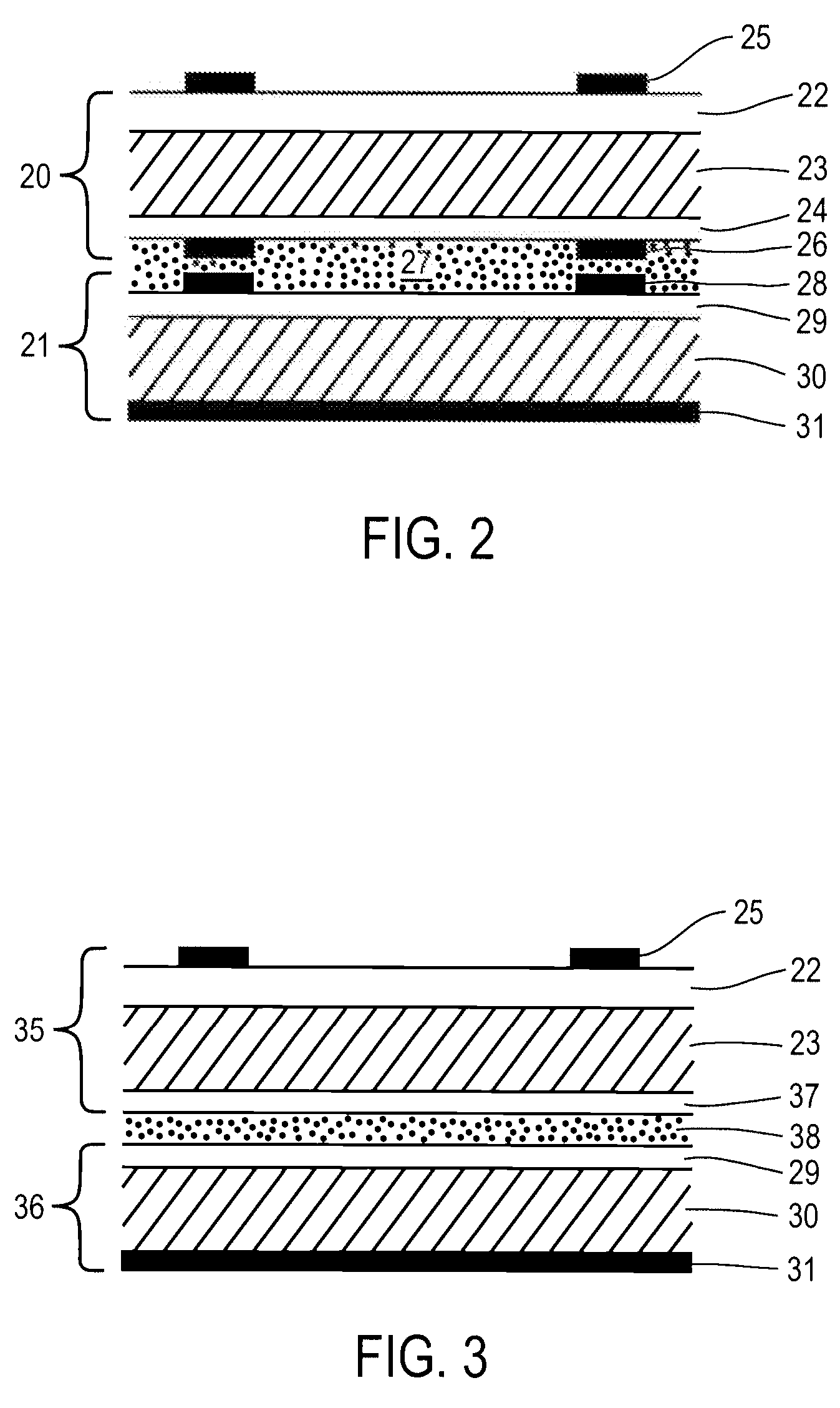
[0031]A large bandgap thin film Cu(In,Ga)(S,Se)2 top cell may be directly fabricated on a bottom cell to form a two-terminal device using the teachings of this invention. In this case, referring to FIG. 5, the base is an already formed bottom cell 50, which may be a thin film CuInSe2 device fabricated on a transparent or non-transparent substrate 51. The general structure of the bottom cell 50 may be “substrate 51 / bottom cell contact 52 / CuInSe2 layer 53 or bottom cell absorber / bottom cell buffer layer 54 / bottom cell TCO layer 55” with an optional finger pattern (not shown) on the bottom cell TCO layer 55. A RuO2 film 56 may be deposited over the bottom cell TCO layer 55. Thickness of the RuO2 film 56 may be in the range of 2-200 nm, preferably 5-100 nm, most preferably 5-20 nm. This film may be deposited by various techniques such as evaporation, sputtering, reactive sputtering, reactive evaporation, activated reactive evaporation, oxidation of Ru films, MOCVD, electrodeposition, in...


PUM


Abstract

The present invention relates to thin film solar cell structures and methods of manufacturing them, particularly tandem cell structures and components thereof. In one aspect there is provided a polycrystalline thin film solar cell structure that is semi-transparent and allows a predetermined wavelength range of light to pass therethrough, in which a bottom semi-transparent conductive layer includes at least one of a ruthenium oxide, an osmium oxide and an iridium oxide. In another aspect there is provided a tandem cell structure in which a top cell bottom contact layer includes at least one of a ruthenium oxide, an osmium oxide and an iridium oxide. In a preferred aspect, the tandem cell structure contains a single contact layer between the absorber layer of the top cell and the absorber layer of the bottom cell. In a particular aspect, this single contact layer is a ruthenium oxide layer.

Description

CLAIM OF PRIORITY [0001]This application claims priority to U.S. Provisional Appln. Ser. No. 60 / 820,323 filed Jul. 25, 2006, and also is a continuation-in-part of U.S. application Ser. No. 11 / 462,685 filed Aug. 4, 2006 entitled “Technique For Preparing Precursor Films And Compound Layers For Thin Film Solar Cell Fabrication”, both of which are incorporated herein in their entirety.FIELD OF THE INVENTION [0002]The present invention relates to thin film solar cell structures and methods of manufacturing them.BACKGROUND [0003]Solar cells are photovoltaic devices that convert sunlight directly into electrical power. The most common solar cell material is silicon, which is in the form of single or polycrystalline wafers. However, the cost of electricity generated using silicon-based solar cells is higher than the cost of electricity generated by the more traditional methods. Therefore, since early 1970's there has been an effort to reduce cost of solar cells for terrestrial use. One way ...

Claims


Application Information

Patent Timeline
IPC IPC(8): H01L31/042H01L31/04
CPCH01L31/022466H01L31/072H01L31/0725Y02E10/543H01L31/0749Y02E10/541H01L31/073
Inventor BASOL, BULENT M.
Owner SOLOPOWER
Why Eureka
Try Eureka