
Array-Processed Stacked Semiconductor Packages

a technology of stacked semiconductors and array processing, which is applied in the direction of semiconductor devices, semiconductor/solid-state device details, electrical apparatus, etc., can solve the problems of increasing the complexity of the product, the cost per functional unit should drop, and the increase of the functional complexity paralleled by the equivalent increase in the reliability of the product, so as to improve the strength of the package

Inactive Publication Date: 2008-01-31
TEXAS INSTR INC
View PDF5 Cites 104 Cited by
  • Summary
  • Abstract
  • Description
  • Claims
  • Application Information

AI Technical Summary

Benefits of technology

[0005]Applicants recognize the need for a fresh concept of achieving a coherent, low-cost method of assembling high lead count, yet low contour devices. The concept includes substrates and packaging methods for stacking devices and package-on-package options as well as assembly options for flip-chip and wire bond interconnections. The device can be the base for a vertically integrated semiconductor system, which may include integrated circuit chips of functional diversity and passive components. The resulting system should have excellent electrical performance, especially speed, and high product reliability. Further, it will be a technical advantage that the fabrication method of the system is flexible enough to be applied for different semiconductor product families and a wide spectrum of design and process variations.
[0007]In another embodiment of the invention, the system includes a distribution of the encapsulation compound so that the compound thickness over the components is about equal to the substrate thickness. A balanced distribution of insulators is thus created, which and thus an overall system with a high degree of robustness against thermomechanical stress and distortion.
[0010]The array is bonded to the next array using solder attachment on the metallization (alternatively, thermo-compression bonding may be used). The reflow of multiple stacked packages occurs at one time for the whole array. To enhance the strength of the package, the substrate (laminate tape) can be glued or bonded to a mold cap; a mask protecting the posts / bondwires would be required for this step. Between two package levels, a single ground plane can be shared.

Problems solved by technology

First, the higher product complexity should largely be achieved by shrinking the feature sizes of the chip components while holding the package dimensions constant; preferably, even the packages should shrink.
Second, the increased functional complexity should be paralleled by an equivalent increase in reliability of the product.
Third, the cost per functional unit should drop with each generation of complexity so that the cost of the product with its doubled functionality would increase only slightly.
Recent applications especially for hand-held wireless equipments, combined with ambitious requirements for data volume and high processing speed, place new, stringent constraints on the size and volume of semiconductor components used for these applications.

Method used


Image

  • Array-Processed Stacked Semiconductor Packages
  • Array-Processed Stacked Semiconductor Packages
  • Array-Processed Stacked Semiconductor Packages

Examples


Embodiment Construction

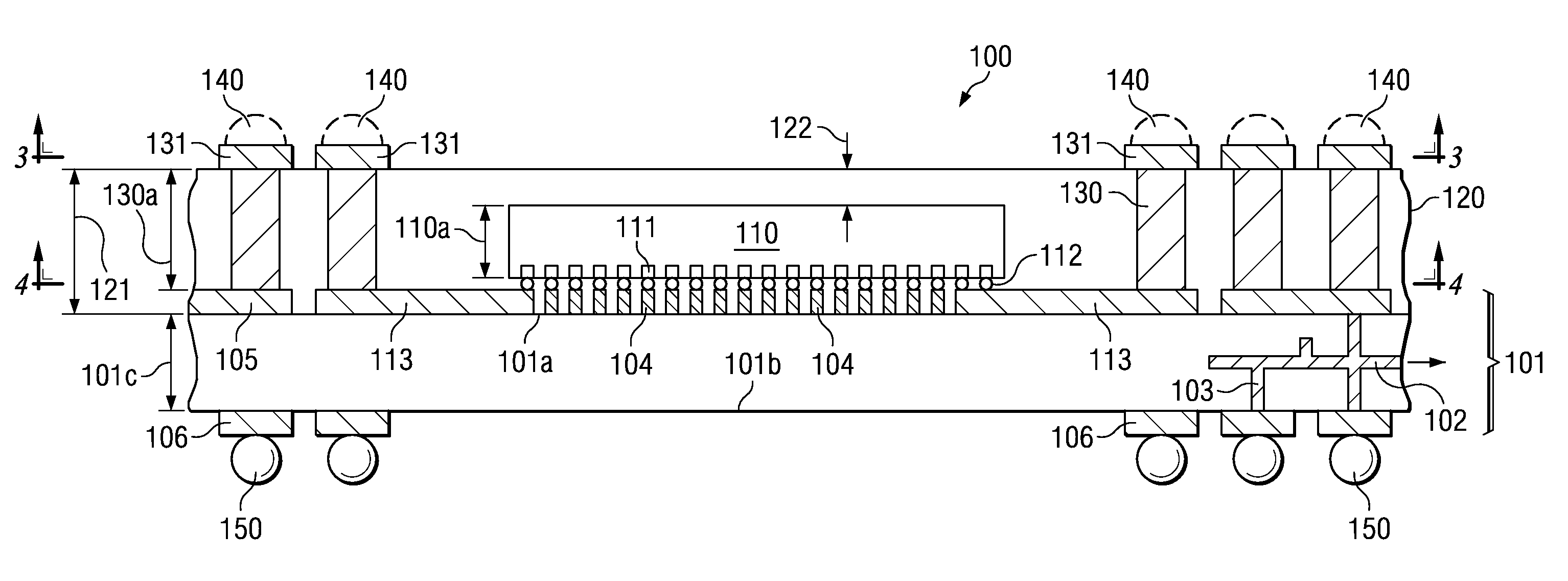
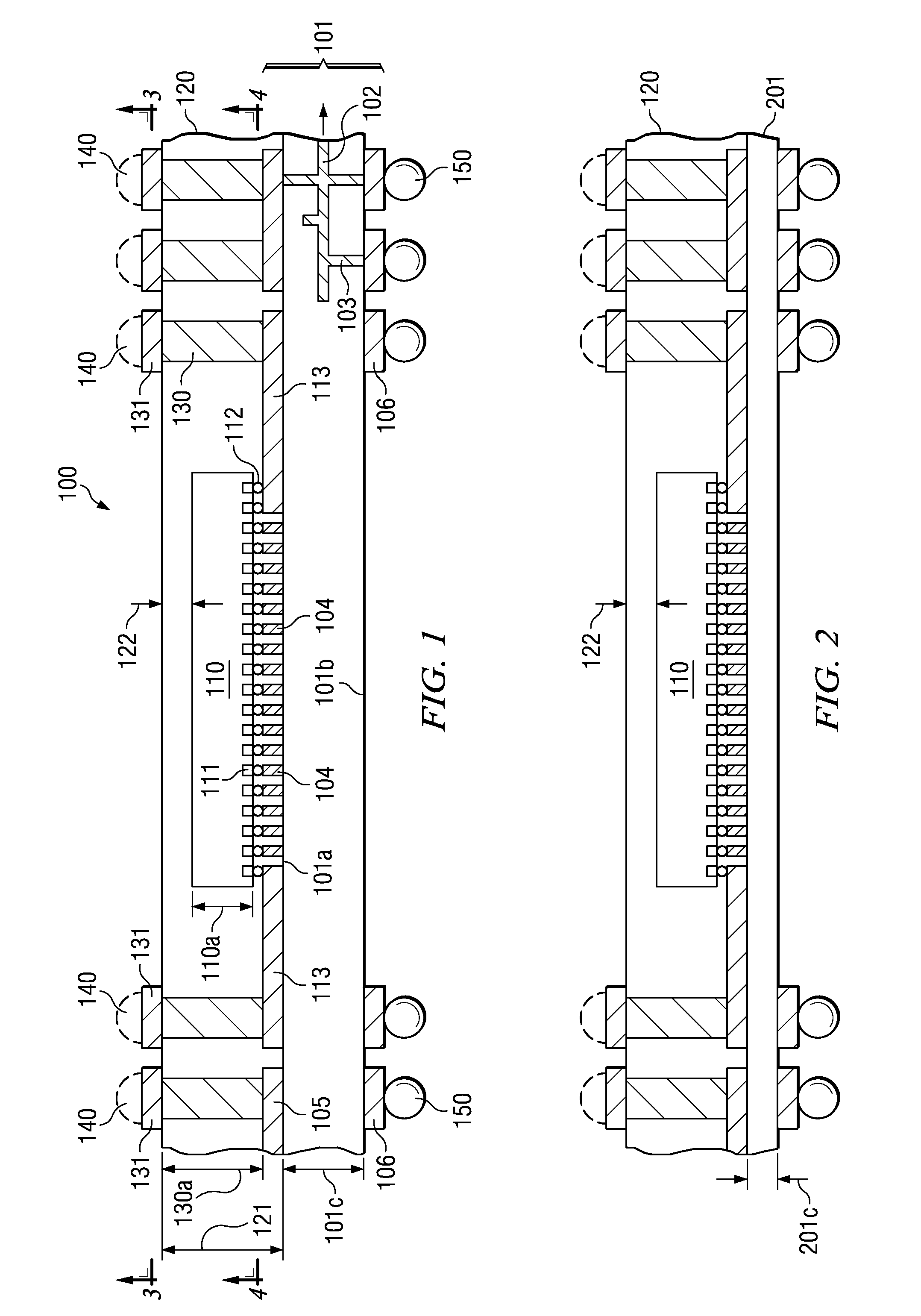
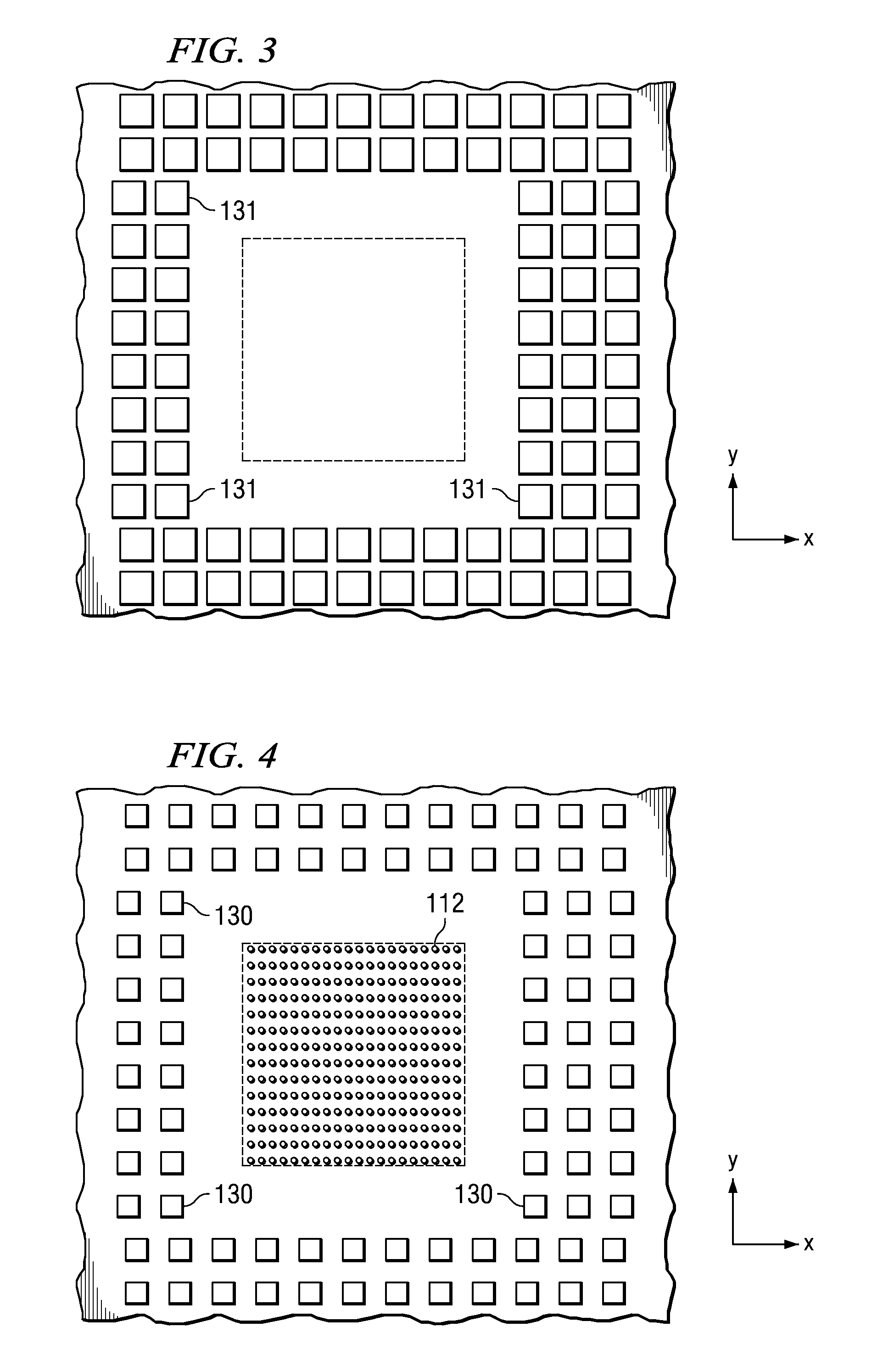
[0029]FIG. 1 illustrates a portion, generally designated 100, of an array shown more fully in FIG. 5. Actually it is, in FIG. 5, the first array of several arrays, which together form a semiconductor system. The first array consists of one or more assembly sites as depicted in FIG. 1; in FIG. 5, each array includes four assembly sites; arrays with considerably higher number of assembly sites can be manufactured. In addition, the sites may be arranged in x-direction as well as in y-direction; the number of sites may be different in x- and y-direction.

[0030]The assembly site depicted in FIG. 1 shows a substrate 101, which has a first surface 101a and a second surface 101b. The substrate is preferably made of a sheet-like insulating material such as polyimide- and / or epoxy-based compounds and has a thickness 101c in the range from about 10 to 1000 μm. Between surfaces 101a and 101b are layers 102 of conductive horizontal lines (preferably copper), and extending from surfaces 101a to su...


PUM


Abstract

One embodiment of the invention is a semiconductor system (1400) of arrays (1401, 1402, etc.) of packaged devices. Each array includes a sheet-like substrate (1411, 1412, etc.) made of insulating material integral with conductive horizontal lines and vertical vias, and terminals on the surfaces. Semiconductor components, which may include more than one active or passive chips, or chips of different sizes, are attached to the substrate; the electrical connections may include flip-chip, wire bond, or combination techniques. Encapsulation compound (1412, 1422, etc.), which adheres to the substrate, embeds the connected components. Metal posts (1431, 1432, etc.) traverse the encapsulation compound vertically, connecting the substrate vias with pads on the encapsulation surface. The pads are covered with solder bodies used to connect to the next-level device array so that a 3-dimensional system of packaged devices is formed.

Description

FIELD OF THE INVENTION[0001]The present invention is related in general to the field of semiconductor devices and processes, and more specifically to array-processed stacked semiconductor packages creating 3-dimensionally interconnected chips.DESCRIPTION OF THE RELATED ART[0002]The long-term trend in semiconductor technology to double the functional complexity of its products every 18 months (Moore's “law”) has several implicit consequences. First, the higher product complexity should largely be achieved by shrinking the feature sizes of the chip components while holding the package dimensions constant; preferably, even the packages should shrink. Second, the increased functional complexity should be paralleled by an equivalent increase in reliability of the product. Third, the cost per functional unit should drop with each generation of complexity so that the cost of the product with its doubled functionality would increase only slightly.[0003]As for the challenges in semiconductor...

Claims


Application Information

Patent Timeline
IPC IPC(8): H01L23/495
CPCH01L23/3121H01L23/5389H01L24/16H01L24/48H01L24/73H01L24/97H01L25/0657H01L25/105H01L25/50H01L2224/13099H01L2224/16H01L2224/4809H01L2224/48091H01L2224/4813H01L2224/48227H01L2224/48472H01L2224/73207H01L2224/73265H01L2224/85951H01L2224/97H01L2924/01005H01L2924/01014H01L2924/01028H01L2924/01029H01L2924/01046H01L2924/0105H01L2924/01079H01L2924/01082H01L2924/014H01L2924/12044H01L2924/14H01L2924/15311H01L2924/15331H01L2924/19041H01L2924/19042H01L2924/19043H01L2224/32225H01L2924/01033H01L2225/1023H01L2225/1058H01L2224/16225H01L2224/32145H01L2924/13034H01L2224/16235H01L2924/00014H01L2224/85H01L2224/83H01L2924/00H01L2924/00012H01L2224/81H01L2924/15747H01L2924/181H01L2224/45144H01L24/45H01L2224/0557H01L2224/05573H01L2224/05571H01L2224/0554H01L2224/06131H01L2224/05599H01L2224/0555H01L2224/0556
Inventor HOWARD, GREGORY E.GUPTA, VIKASEDWARDS, DARVIN R.
Owner TEXAS INSTR INC
Learn More