Process for Producing Light Absorbing Layer for Chalcopyrite Type Thin-Film Solar Cell

a technology of chalcopyrite and light absorbing layer, which is applied in the direction of climate sustainability, final product manufacturing, basic electric elements, etc., can solve the problems of poor adhesion between the light absorbing layer and the electrode layer, difficult to achieve the desired single cigs layer, and poor adhesion between the mo electrode layer and metal ga interface, etc., to achieve positive the effect of photoelectric conversion

Inactive Publication Date: 2008-02-14
HONDA MOTOR CO LTD
View PDF7 Cites 18 Cited by
  • Summary
  • Abstract
  • Description
  • Claims
  • Application Information

AI Technical Summary

Benefits of technology

[0029] According to the process for producing the light absorbing layer for the chalcopyrite type thin-film solar cell of the present invention, in the first selenization step having a relatively low temperature, the interior of the airtight space is preheated and an atmosphere in the airtight space is stabilized by introducing hydrogen selenide gas. In the second selenization step having a relatively high temperature, Se components are extracted into the light absorbing layer and Ga components are diffused in the light absorbing layer. In the third

Problems solved by technology

Three components other than Se tend to be alloyed or the In layer tends to be deposited on the Cu—Ga layer, resulting in difficulty in transformation into the desired single CIGS layer.
However, it is known that adhesion is poor on the interface of

Method used


Image

  • Process for Producing Light Absorbing Layer for Chalcopyrite Type Thin-Film Solar Cell
  • Process for Producing Light Absorbing Layer for Chalcopyrite Type Thin-Film Solar Cell
  • Process for Producing Light Absorbing Layer for Chalcopyrite Type Thin-Film Solar Cell

Examples


example 1

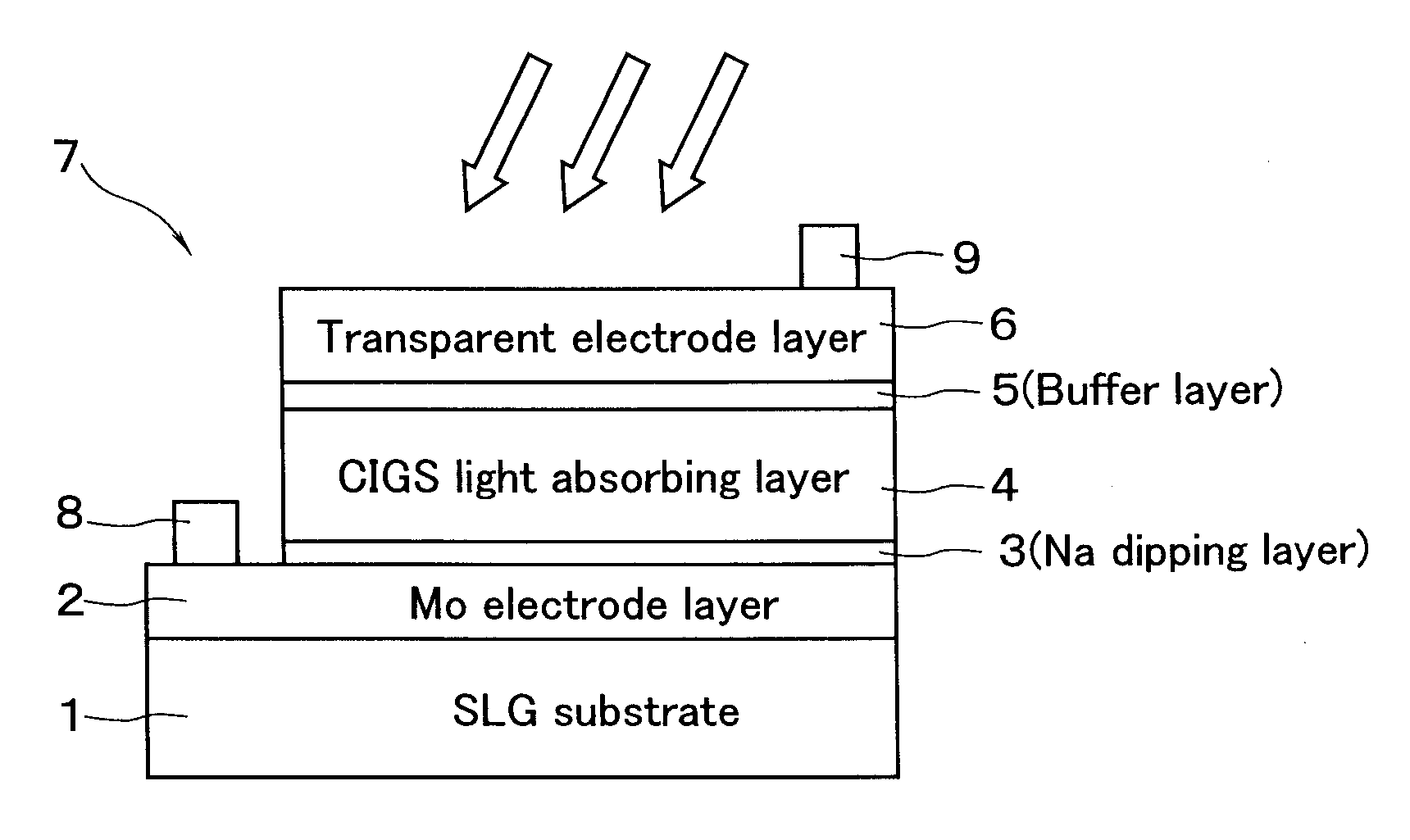
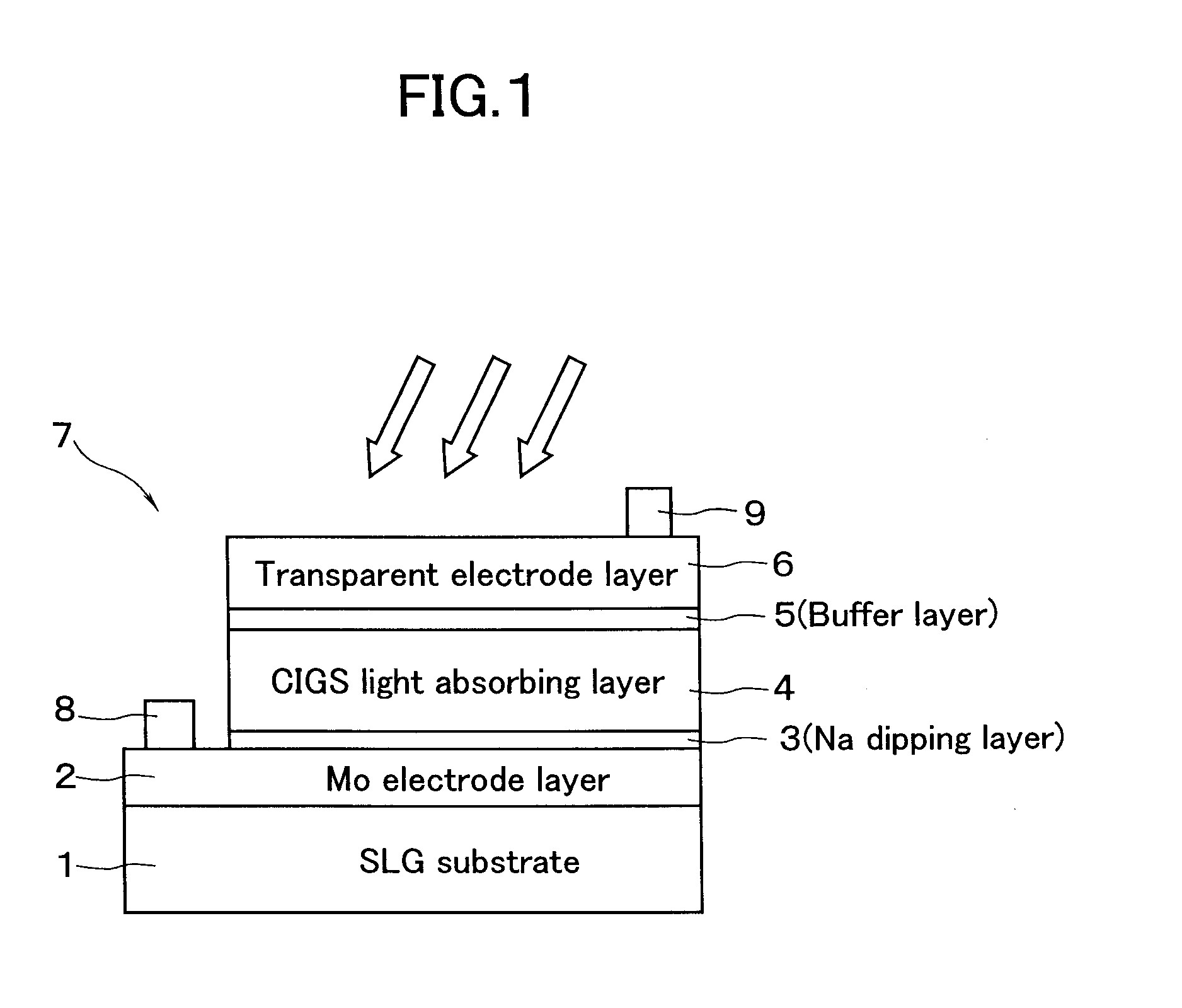
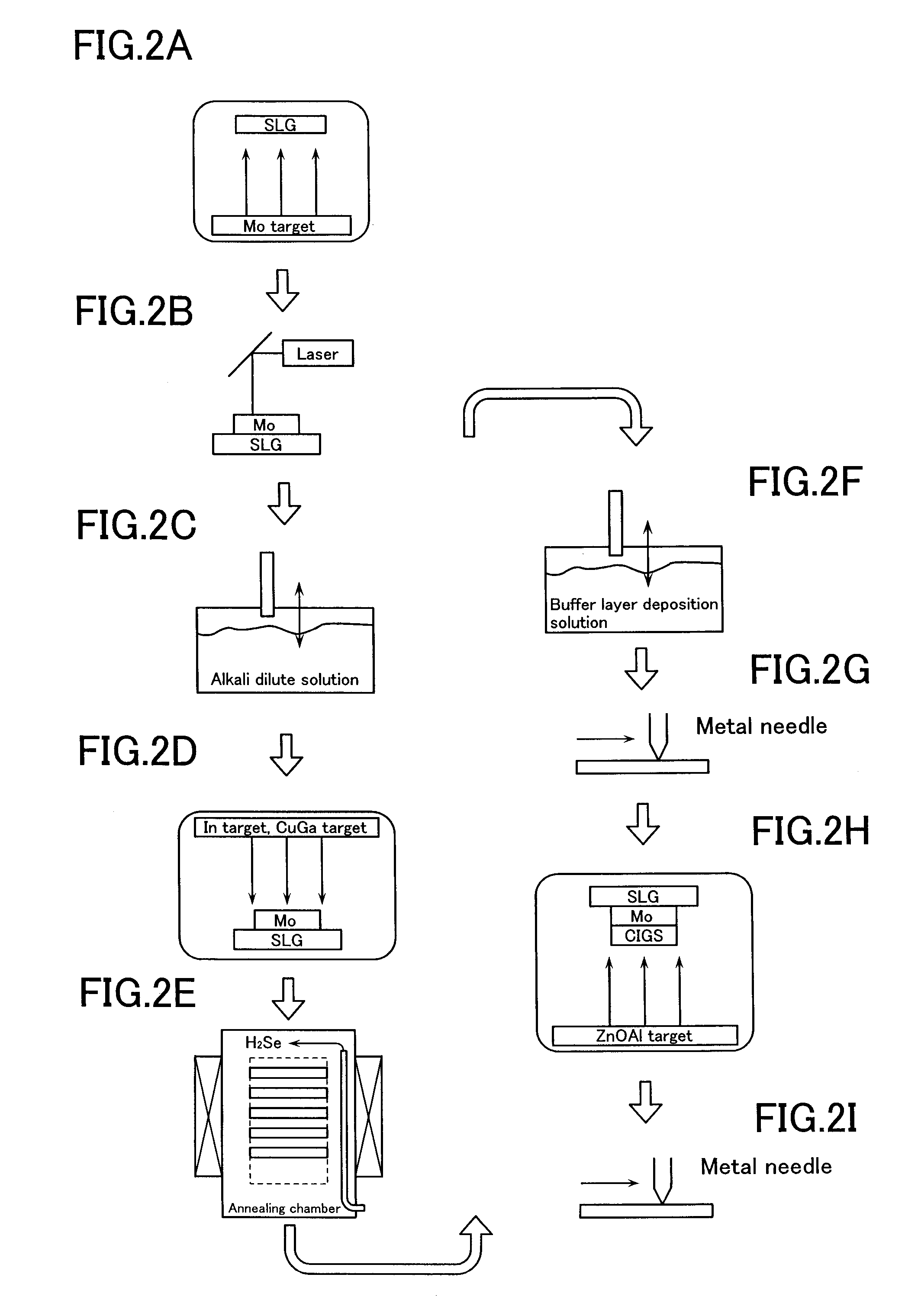
[0051] When the light absorbing layer 4 (FIG. 1) is produced, the predetermined number of glass substrates 1c are accommodated in the heat treatment chamber 40 shown in FIG. 4. The In metal layer and the Cu—Ga alloy layer have been superimposed on the substrate 1c by using the inline sputter deposition device 38 (FIG. 3). Then, selenization is performed according to a temperature profile shown in FIG. 5.

[0052] In other words, the interior of the process tube 46 is heated by the heaters 41 so as to range from room temperature to 250° C., more preferably to range from 30° to 150° C. In a state in which the interior of the process tube 46 is kept at a predetermined temperature within this range, hydrogen selenide (H2Se) gas is introduced from the nozzle holes 48 of the gas inlet tube 47 with a predetermined flow rate for time t1 while keeping the interior of the process tube 46 at a reduced pressure of 50 to 95 kPa in response to the operation of the evacuating mechanism. The above fi...

example 2

[0059] As in Example 1, the glass substrates 1c on which the In metal layer and the Cu—Ga alloy layer are superimposed are accommodated in the heat treatment chamber 40. Then, selenization is performed according to a temperature profile shown in FIG. 6. The temperature profile of this example is different from that of FIG. 5 in that H2Se gas is supplied with relatively a low flow rate immediately after the first selenization step and the H2Se gas is continuously supplied without interruption in the second selenization step after the temperature increases to 250° to 450° C. In FIG. 6, time t5 represents the second selenization step including heating-up time immediately after the first selenization step.

[0060] In the second selenization step having longer Se extraction time, the flow rate of continuously supplied H2Se gas per unit time is set lower than that of the second selenization step of Example 1. In this second selenization step, Se components can be extracted into the light a...


PUM


Abstract

A process for producing a light absorbing layer for thin-film solar cell that possesses a film structure having a constituent component of chalcopyrite compound (Cu(In+Ga)Se2) uniformly distributed thereinside. There is provided a process for producing a light absorbing layer, including the precursor forming step of superimposing on an Mo electrode layer, adjacent to the electrode layer, an In metal layer and a Cu—Ga alloy layer according to sputtering technique; a first selenization step of, while accommodating precursor-provided substrate in an airtight space, introducing hydrogen selenide gas in the airtight space conditioned so as to range from room temperature to 250° C.; a second selenization step of additionally introducing hydrogen selenide gas in the airtight space heated so as to range from 250° to 450° C.; a third selenization step of, while causing the hydrogen selenide gas having been introduced up to the second selenization step to remain, heating the interior of the airtight space so as to range from 450° to 650° C. and, within this range of temperature, performing heat treatment of the substrate; and a cooling step of cooling the substrate after the heat treatment.

Description

TECHNICAL FIELD [0001] The present invention relates to a process for producing a light absorbing layer for a chalcopyrite type thin-film solar cell in which the light absorbing layer includes a chalcopyrite compound layer. BACKGROUND ART [0002] Of various solar cells broadly classified into silicon solar cells, thin-film solar cells, and compound solar cells, thin-film solar cells have been commercialized as optical devices using thin-film technology because its manufacturing process is simple and achieves low energy. A chalcopyrite type thin-film solar cell belongs to thin-film type and comprises a CIGS layer made of a chalcopyrite compound (Cu(In+Ga)Se2:CIGS) as a p-type light absorbing layer. It is known that the light absorbing layer made of such a compound enables a solar cell to have high photoelectric conversion efficiency particularly when the light absorbing layer is combined with a glass substrate containing an alkali metal such as soda lime glass. Research and developmen...

Claims


Application Information

Patent Timeline
IPC IPC(8): H01L31/0272H01L21/363H01L31/032H01L31/04
CPCY02E10/541H01L31/0322Y02P70/50
Inventor KUME, TOMOYUKIKOMARU, TAKASHI
Owner HONDA MOTOR CO LTD
Why Eureka
Try Eureka