

Optical Waveguide Module
- Summary
- Abstract
- Description
- Claims
- Application Information
AI Technical Summary
Benefits of technology
Problems solved by technology
Method used
Image

Examples
first embodiment
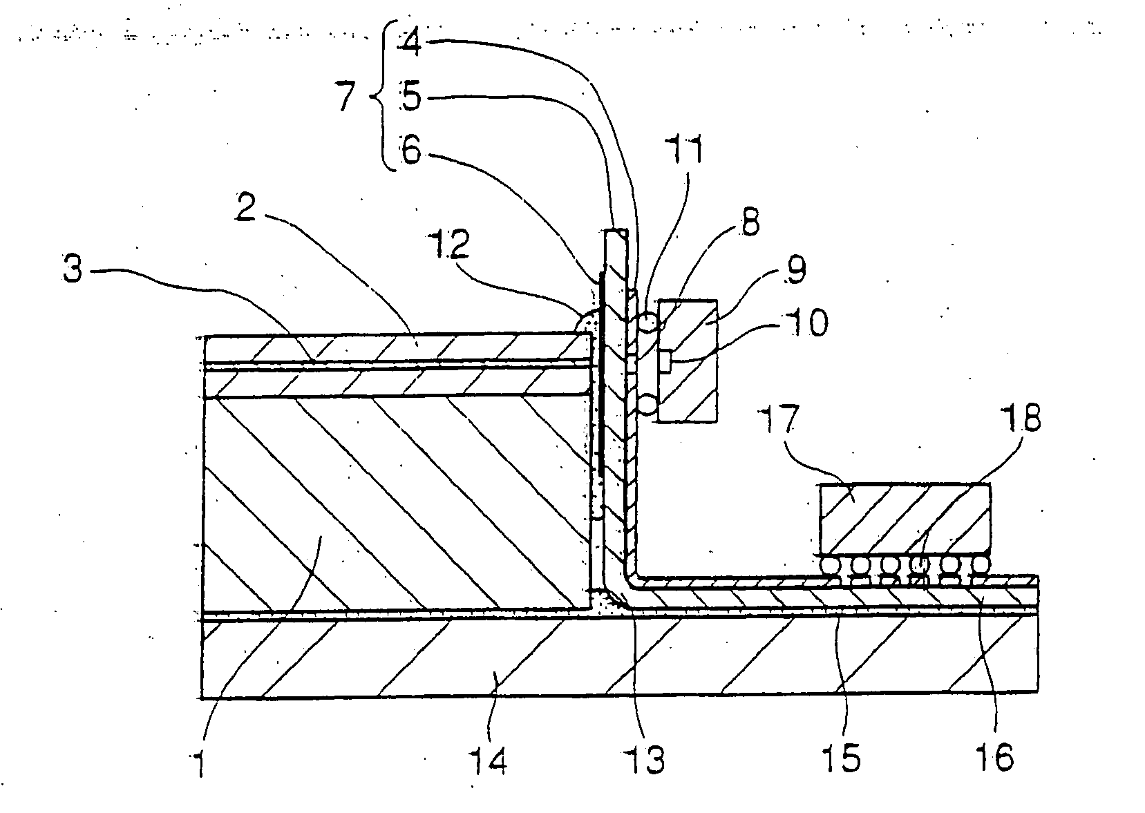
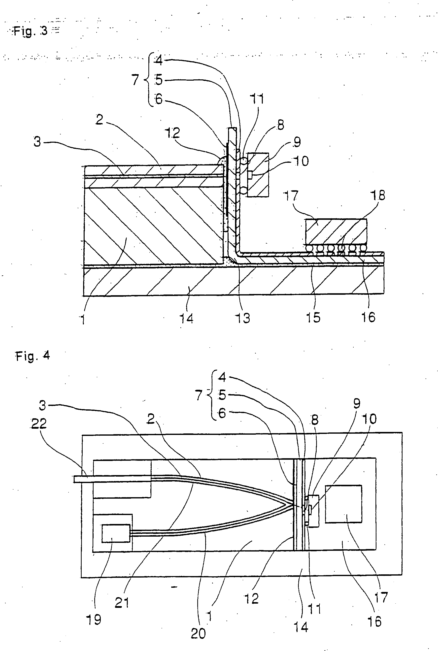
[0031]FIG. 3 is a view showing the configuration of optical coupling between an optical waveguide and a light-receiving element of the optical waveguide module of the present invention. FIG. 3 is a sectional view taken along a cutting surface including the optical axis of the core of the optical waveguide.
[0032] In the present embodiment, wiring board 7 having a thickness of 50 μm is composed of base member 5, surface electrical wiring 4, and filter film (wavelength filter in a film shape) 6. Base member 5 has transparency with respect to light of wavelength λ1 (for example, 1.55 μm) that can be received by light-receiving element 9. Filter film 6 is formed on the rear surface of surface electrical wiring 4, and has characteristics for passing light of wavelength λ1 that can be received by light-receiving element 9 and for reflecting light of other wavelengths. Aperture 8 having a diameter of 100 μm, which is larger than a diameter of core 3 of the optical waveguide, is formed in su...
second embodiment
[0044]FIG. 5 shows the optically coupled configuration of the optical waveguide and light-receiving element in the optical waveguide module according to the present invention. FIG. 5 is a sectional view taken along a cutting surface including the optical axis of the core of the optical waveguide.
[0045] In this embodiment, wiring board 32 having a thickness of 50 μm is composed of base member 31 and surface electrical wiring 30. Base member 31 has transparency with respect to light of wavelength λ1 (for example, 1.55 μm) that can be received by light-receiving element 9. Aperture 33 having a diameter of 100 μm, which is larger than a diameter of core 3 of optical waveguide 2, is formed in surface electrical wiring 30 of wiring board 32. Main surface-incidence type light-receiving element 9 is flip-chip mounted on surface electrical wiring 30 using gold stud bumps 11 having a height of approximately 20 μm. Light-receiving region 10 of this light-receiving element 9 is arranged to face...
third embodiment
[0049]FIG. 7 shows the optically coupled structure of the optical waveguide and light-receiving element in the optical waveguide module according to the present invention. FIG. 7 is a sectional view taken along a cutting surface including the optical axis of the core of the optical waveguide.
[0050] In the present embodiment, wiring board 42 having a thickness of 50 μm is composed of base member 41 and surface electrical wiring 40. Base member 41 has transparency with respect to light of wavelength λ1 (for example, 1.55 μm) that can be received by light-receiving element 9. Aperture 43 having a diameter of 200 μm, which is sufficiently larger than a diameter of core 3 of optical waveguide 2, is formed in surface electrical wiring 40 of wiring board 42. Main surface-incidence type light-receiving element 9 is then flip-chip mounted on surface electrical wiring 40 using gold stud bumps 11 having a height of approximately 20 μm. Light-receiving region 10 of this light-receiving element ...
PUM
 Abstract
Description
Claims
Application Information