
Integrated circuit package with a heat dissipation device and a method of making the same

a technology of integrated circuits and heat dissipation devices, which is applied in the direction of semiconductor devices, semiconductor device details, electrical apparatus, etc., can solve the problems of limiting the design of microelectronic devices, limiting the performance level, and new-age devices such as high-power amplifiers and multi-chip modules, which radiate particularly large amounts of heat. , to achieve the effect of dissipating generated heat spikes and improving the electrical reliability of integrated circuits

Inactive Publication Date: 2008-02-21
POLARIS INNOVATIONS
View PDF17 Cites 57 Cited by
  • Summary
  • Abstract
  • Description
  • Claims
  • Application Information

AI Technical Summary

Benefits of technology

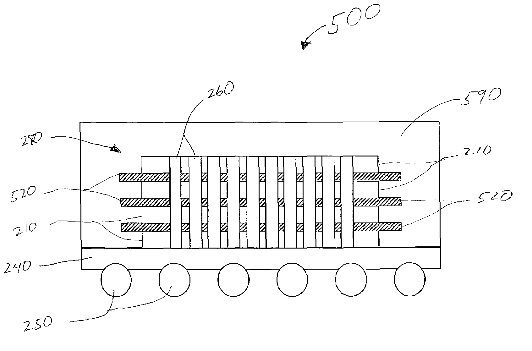
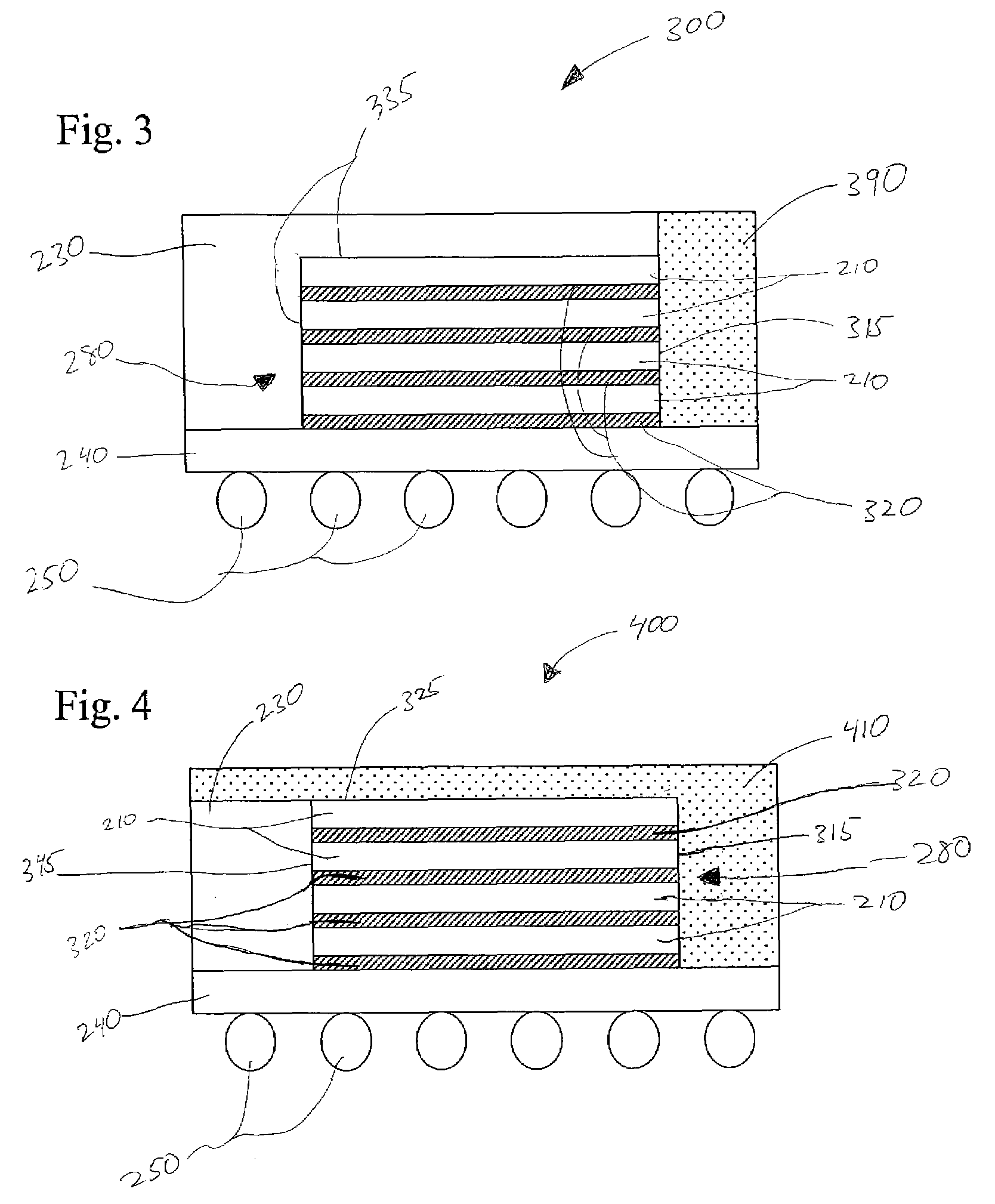
[0017]Another believed advantage of the present invention is the invention's ability to dissipate generated heat spikes that are often associated with electrical load spikes in the integrated circuits within die stack assembly, especially load spikes in the lowermost and innermost areas of the die stack assembly. As higher and higher frequencies are demanded of integrated circuits, more and more heat will be generated and need to be dissipated to improve electrical reliability of the integrated circuits. A vertical heat dissipation device attached to the side of a heat package may overcome the above drawbacks.

Problems solved by technology

However, small, closely packed features dissipate large amounts of heat which may limit performance levels.
Temperature control has thus emerged as a limiting factor in the design of microelectronic devices.
New-age devices, such as high-power amplifiers and multi-chip modules, radiate particularly large amounts of heat.
Failure to effectively conduct heat away generally leaves these devices operating at high temperatures, ultimately resulting in decreased performance and reliability.
Additionally, increased demand for downsizing modules accommodating microelectronic components including integrated circuit devices complicates both the need to remove excessive heat generated by integrated circuit devices and how to accomplish heat removal within an increasingly limited area.
Furthermore, many integrated circuit devices including memory devices and chip type circuit components are mounted on a printed circuit board so that the number of components mounted on a module has a tendency to increase and resulting in decreased surface area available for conventional heat sinks.
However, any cover cap or encapsulant above the integrated circuit increases the thermal resistance path to an ambient environment and hence the operation temperature of the integrated circuit, and the resulting heat density of the multi-chip module.
Nevertheless, one problem with the preferential heat dissipation pathway travelling in the vertical direction through the package, especially in die stack packages, is that the top most integrated circuit will be cooled much better than any underlying integrated circuits.
Of course such a preferential heat dissipation pathway means that in order to cool the lower most integrated circuit within a stack, the heat must travel through the entire stack and any intermediate layers to be discharged through the upper surface and into the ambient surroundings, likely resulting in particular difficulties for sufficiently cooling the lower most integrated circuit within a stack.
Another potential drawback of having the heat transfer pathway preferentially travel from the bottom most integrated circuit through the die stack and to the top most integrated circuit is that each succeeding upper integrated circuit may be heated up by the lower integrated circuit as heat passes from a lower integrated circuit to an above lying integrated circuit and so on up the die stack.
Moreover, there are some uses of stacked integrated circuits which do not permit the upper most surface to function simultaneously as a heat dissipation surface available for mounting a heat spreader.
For example a sensor array type integrated circuit may not permit a heat sink attached to the upper surface of an integrated circuit package.
Furthermore, any intermediate interfaces between integrated circuits often contribute to the overall thermal resistance of a die stack thereby limiting the heat dissipation potential of the bottom most integrated circuit and so on through the stack up to the top most integrated circuit.

Method used


Image

  • Integrated circuit package with a heat dissipation device and a method of making the same
  • Integrated circuit package with a heat dissipation device and a method of making the same
  • Integrated circuit package with a heat dissipation device and a method of making the same

Examples


Embodiment Construction

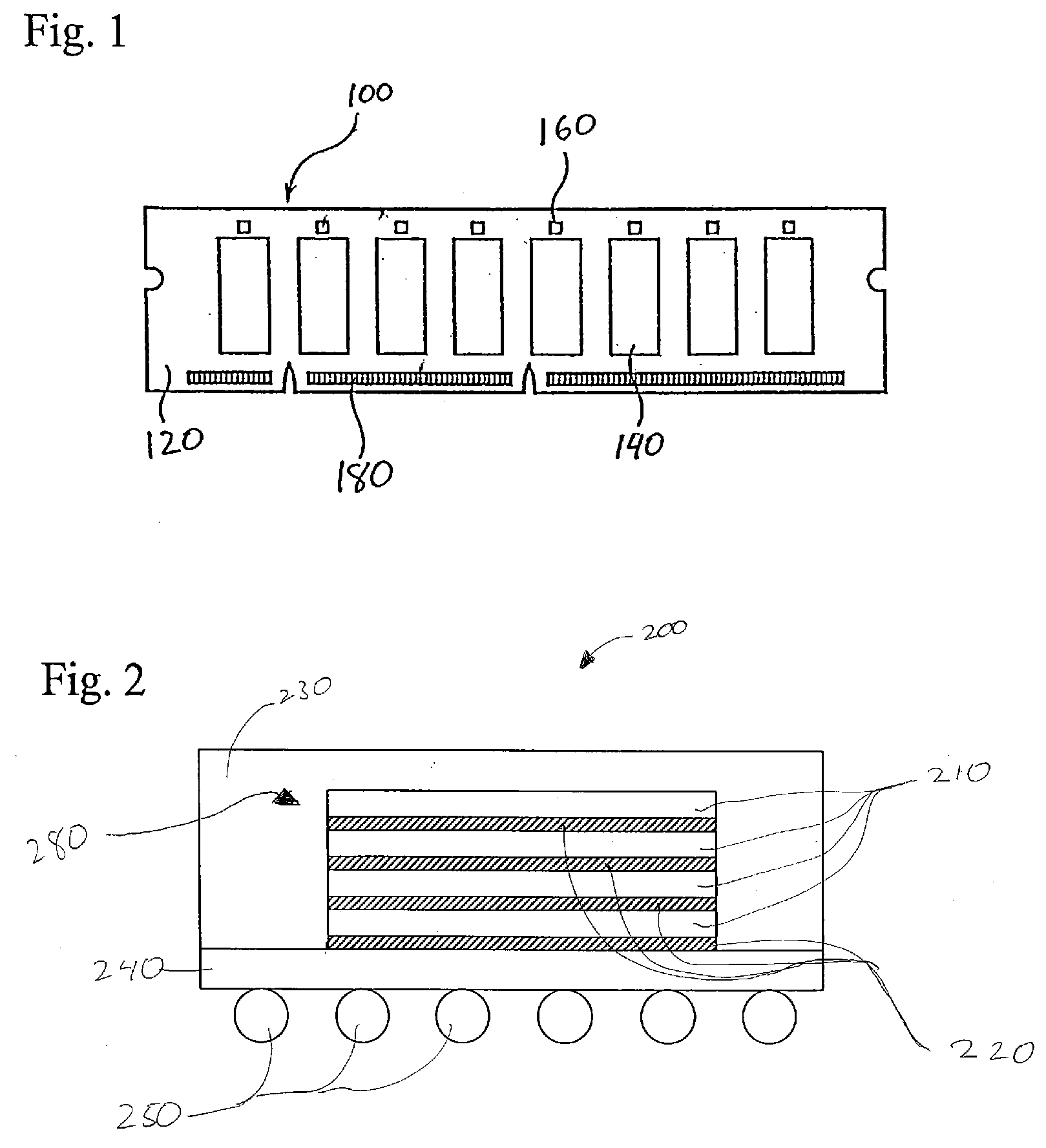
[0036]These aspects of the present invention may provide particular advantages for improved heat transfer through packages for an integrated circuit assembly. Turning now to FIG. 1, a diagrammatic plan view of a multi-chip module, in this case a conventional memory module 100 is shown. The memory module shown is just one example of where packages of integrated circuit assemblies may be employed. The memory module 100 comprise packages for an integrated circuit assembly 140. The packages 140 may comprise integrated circuit devices such as memory devices, that may be DRAM or Dynamic Random Access Memory. A memory module 100 conventionally has a plurality of packages for integrated circuit assemblies 140. Next to the packages 140 may be other devices 160 such as termination resistors, capacitors, and the like. These devices 160 are also placed on the printed circuit board 120.

[0037]The printed circuit board 120 has an array of contact pads 180 provided along a side edge of each face of...


PUM


Abstract

Integrated circuit assembly including a die stack assembly having a heat dissipation device thermally coupled to a lateral of surface the die stack assembly. The die stack assembly includes a plurality integrated circuits placed on each other. In another embodiment a heat dissipation device comprising an encapsulant is thermally coupled to and surrounds a die stack assembly that includes a plurality of integrated circuits placed on each other. At least one heat conducting intermediate layer between integrated circuits is thermally coupled to the heat dissipation device.

Description

BACKGROUND OF THE INVENTION[0001]1. Field of the Invention[0002]The present invention relates generally to the field of integrated circuit devices and more particularly to packages for integrated circuits where the package includes a heat sink. The present invention also relates to a method of making a package for integrated circuits including a method of forming a heat dissipation device.[0003]2. Description of the Related Art[0004]The performance levels of microelectronic devices, for example integrated circuits, power amplifiers, etc., are continually increasing to keep pace with the demands of modern technology. Performance levels such as clock speed are closely tied to the number and density of features, for example transistors, patterned onto the microelectronic device. Faster processing by the microelectronic device demands faster clock speeds. Faster clock speeds, in turn, mean more switching and power dissipation per unit time. The performance levels of microelectronic devi...

Claims


Application Information

Patent Timeline
IPC IPC(8): H01L23/34H01L21/00
CPCH01L25/0657H01L2225/06541H01L2225/06562H01L2224/32225H01L2225/06589H01L2924/15311H01L2224/32145H01L2225/06586H01L2924/181H01L2924/00012
Inventor WOLTER, ANDREASHEDLER, HARRYGEORGI, MATTHIAS
Owner POLARIS INNOVATIONS
Learn More