Plasma display device and light emitting device

Inactive Publication Date: 2008-02-28
HITACHI LTD +1
View PDF5 Cites 7 Cited by
  • Summary
  • Abstract
  • Description
  • Claims
  • Application Information

AI Technical Summary

Problems solved by technology

In other words, since CMS has a low emission efficiency with respect to the Xe2 molecular line at a wavelength of 172 nm to be increased with respect t

Method used


Image

  • Plasma display device and light emitting device
  • Plasma display device and light emitting device
  • Plasma display device and light emitting device

Examples


first embodiment

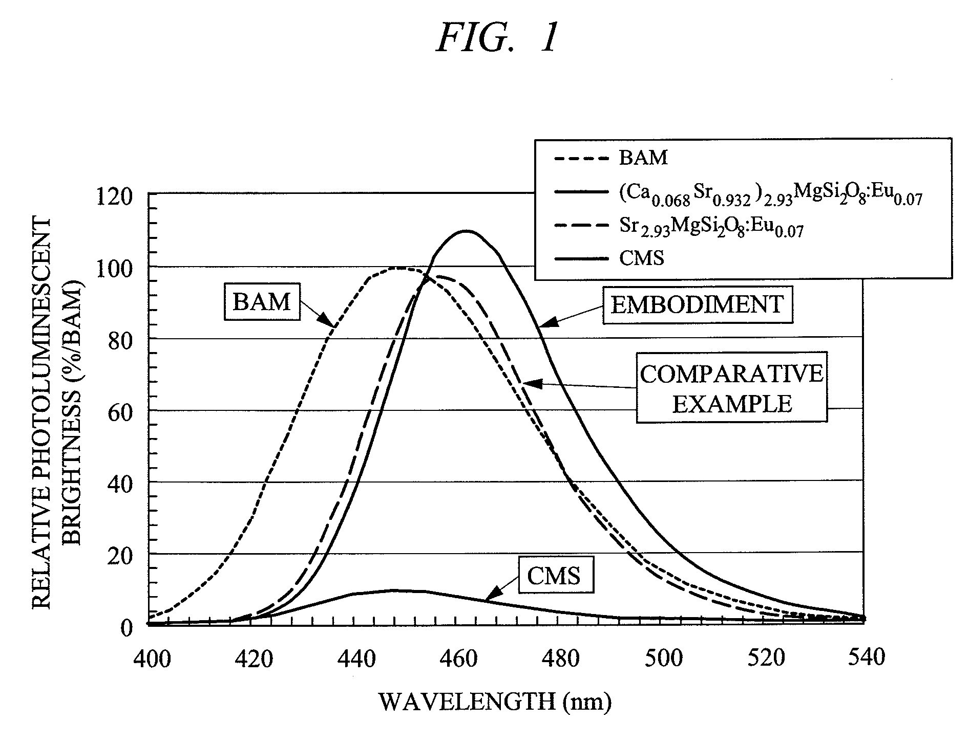
[0112]To produce a plasma display panel as a first embodiment of the present invention, first, an Eu-activated silicate phosphor as an essential constituent member of the present invention is synthesized.

[0113]For the synthesis of a phosphor having a composition formula (Ca0.034Sr0.966)2.93MgSi2O8:Eu0.07, first, 0.100 g (1.00 mmol) of CaCO3, 4.178 g (28.30 mmol) of SrCO3, 0.962 g (10.00 mmol) of MgCO3, 1.202 g (20.00 mmol) of SiO2, 0.1230 g (0.350 mmol) of Eu2O3, and 0.392 g (4.00 mmol) of NH4Br as a flux are respectively weighed and fully mixed in an agate mortar. Thereafter, the obtained mixture is charged into a heat-stable vessel and heated for 3 hours at 1000° C. in the atmosphere. Thereafter, it is further heated for 3 hours at 1200° C. in a reducing atmosphere. The obtained product is pulverized, washed with water and dried so as to obtain a silicate phosphor of the above composition.

[0114]Next, for the synthesis of a phosphor (Ca0.068Sr0.932)2.93MgSi2O8 :Eu0.07, in the same ...

second embodiment

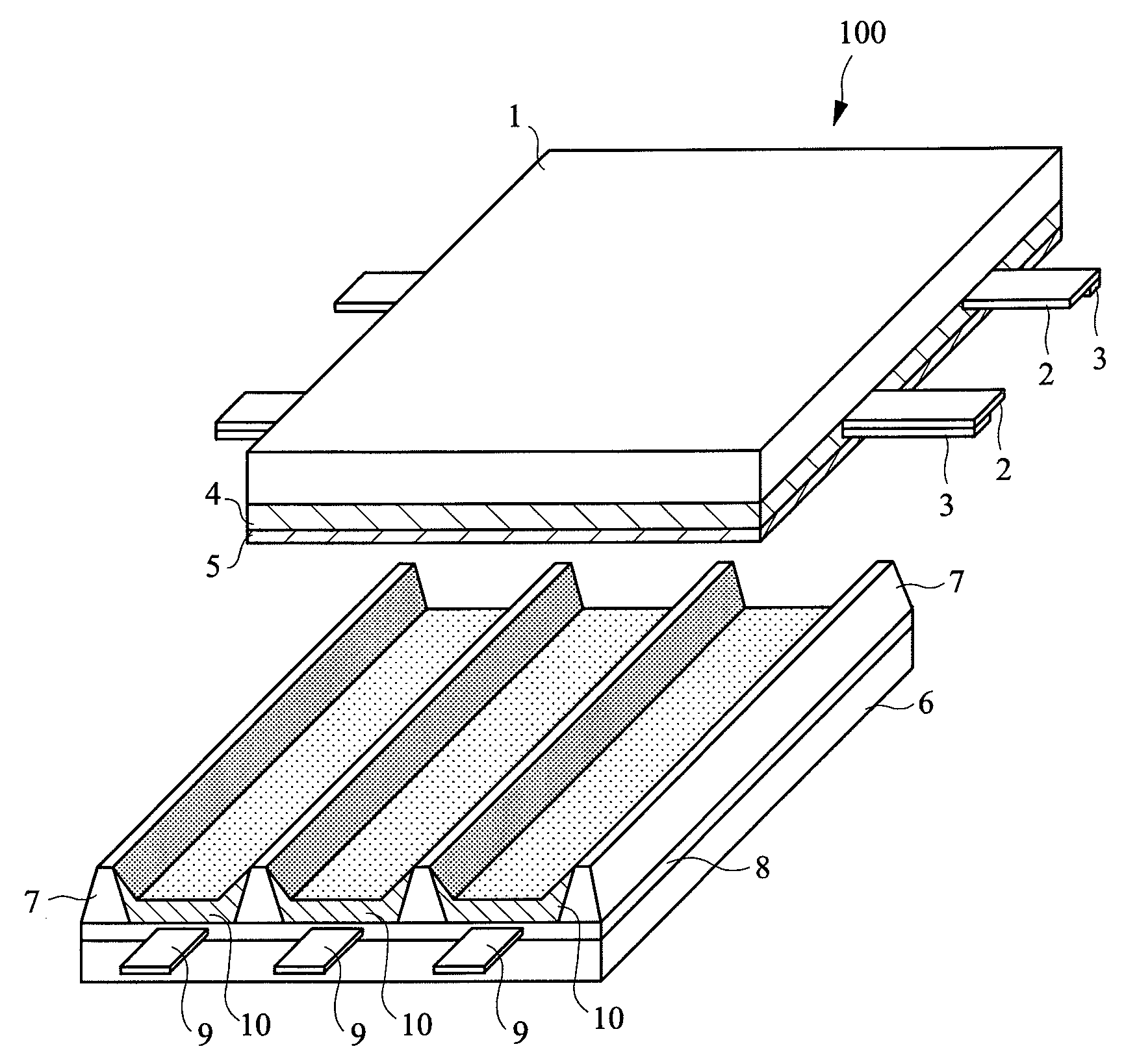
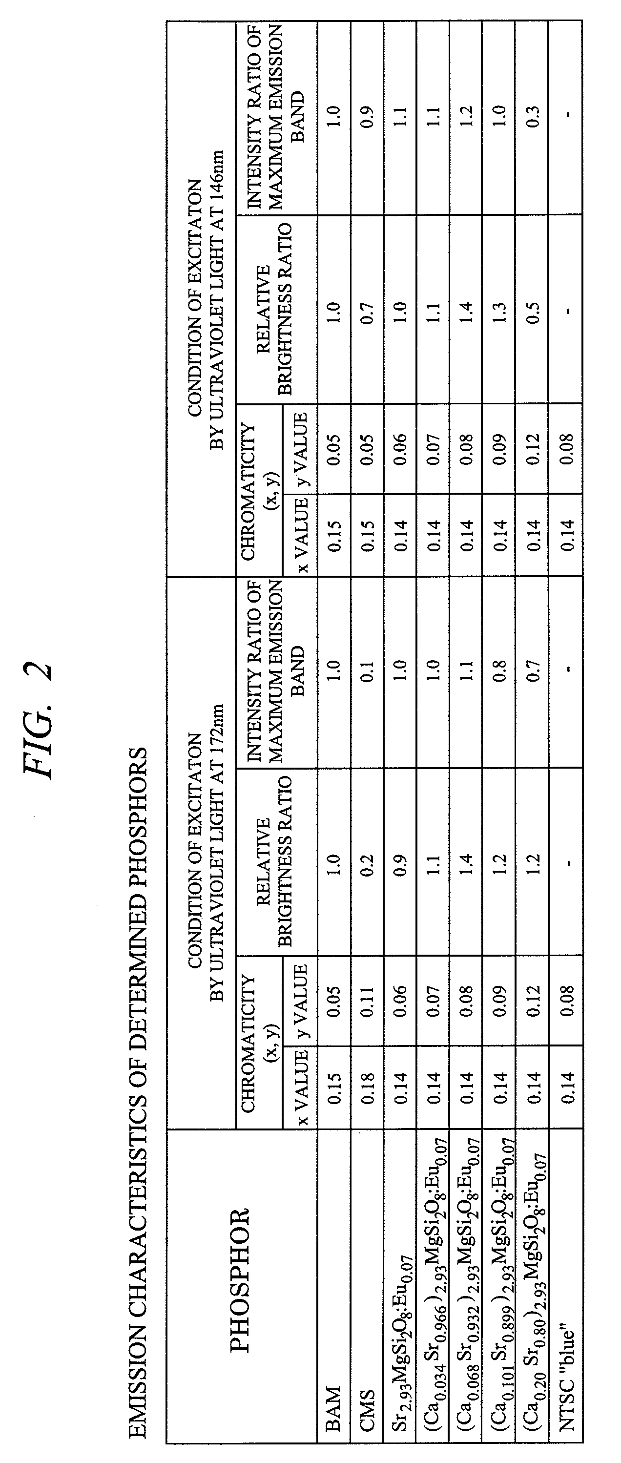
[0118]For evaluating the novel Eu-activated silicate phosphors of the present invention as well as the characteristics and the reliability of the PDP using the same as the light emitting device of the present invention, as two phosphors to configure the phosphor layer, (Ca0.068Sr0.932)293MgSi2O8:Eu0.07 as the silicate phosphor of the present invention synthesized in the first embodiment and BAM as the conventional blue-emitting phosphor are used and the plasma display panel (PDP) 100 shown in FIGS. 5 to 8 is prepared. FIG. 5 is an exploded perspective view of main parts showing the structure of the PDP of an embodiment of the present invention. Moreover, FIGS. 6, 7, 8 are cross-sectional views showing main parts of the structure of PDP according to an embodiment of the present invention.

[0119]For preparing the PDP 100, first, after forming the address electrode 9 made of Ag or the like, and the dielectric layer 4 made of a glass-based material on the rear substrate 6, a barrier rib ...

third embodiment

[0130]Using phosphors of three colors of the novel Eu-activated silicate blue-emitting phosphor of the present invention (Ca0.068Sr0.932)2.93MgSi2O8:Eu0.07, a red-emitting phosphor, and a green-emitting phosphor, a color PDP is prepared as a light emitting device capable of color display.

[0131]The structure of the color PDP of the present embodiment is same as the PDP 100 shown in FIGS. 5 to 8, but it is different therefrom in that the phosphor layers corresponding to the three color light emission are provided like stripes successively over a front surface of the display region for enabling the color display. Therefore, since details of the other configuration and the method of preparation are same as those of the second embodiment, the description thereof is omitted.

[0132]In the preparation process in the second embodiment, the phosphor layers 10 corresponding to color emission of red (R), green (G), blue (B), respectively are formed on the barrier ribs 7 so as to cover the groove...


PUM


Abstract

A plasma display panel including a discharge gas for generating ultraviolet light as a result of electric discharge, and a phosphor layer containing a phosphor for emitting light upon excitation by ultraviolet light is provided. The phosphor contains a novel Eu-activated silicate phosphor represented by (CaxM11-x)3-e.M2.Si2O8: Eue. In the formula, M1 is at least one element selected from the group consisting of Sr and Ba; M2 is at least one element selected from the group consisting of Mg and Zn; x is the mole fraction of the component Ca satisfying the condition of 0<x≦0.2, and e is the mole fraction of Eu satisfying the condition of 0.001≦e≦0.2.

Description

CROSS-REFERENCE TO RELATED APPLICATION[0001]The present application claims priority from Japanese Patent Application No. JP 2006-230595 filed on Aug. 28, 2006, the content of which is hereby incorporated by reference into this application.TECHNICAL FIELD OF THE INVENTION[0002]The present invention relates to a light emitting device, in particular, it relates to a light emitting device such as Plasma Display Panel (PDP) using an Eu-activated silicate phosphor which emits light by being excited by ultraviolet light in the vacuum ultraviolet region.BACKGROUND OF THE INVENTION[0003]In recent years, demands to reduce the thickness of display devices represented by television sets and monitors for personal computers for saving installation space has been increased. As a display device capable of being slimmed, a plasma display device for displaying images using a plasma display panel with a driver device which drives the PDP, which is thinner than the cathode ray tube as the light emittin...

Claims


Application Information

Patent Timeline
IPC IPC(8): H01J1/62H01J17/49C09K11/59H01J11/12H01J11/22H01J11/24H01J11/26H01J11/34H01J11/36H01J11/38H01J11/40H01J11/42H01J11/50
CPCC09K11/7734H01J11/42H01J11/12C09K11/77342
Inventor OAKU, HITOSHISAKUMA, HIROTAKAOKAZAKI, CHOICHIRO
Owner HITACHI LTD
Why Eureka
Try Eureka