
Insulator film, manufacturing method of multilayer wiring device and multilayer wiring device

a manufacturing method and wiring device technology, applied in the direction of semiconductor/solid-state device manufacturing, basic electric elements, electric apparatus, etc., can solve the problems of increasing the dielectric constant, and reducing the negative effect, preventing the increase of the dielectric constant, and high film strength

Active Publication Date: 2008-02-28
FUJITSU LTD
View PDF8 Cites 16 Cited by
  • Summary
  • Abstract
  • Description
  • Claims
  • Application Information

AI Technical Summary

Benefits of technology

[0020] According to these aspects of the present invention, it is possible to obtain a multilayer wiring device having a low-dielectric-constant insulator film that has a high film strength and can prevent increase of its dielectric constant due to moisture absorption. By this, it is possible to prevent delay in the device response speed caused by parasite capacity increase in the multilayer wiring device as well as the decrease of its device reliability. It is also possible to improve the yield and provide a multilayer wiring device with higher reliability, by restraining thermal history through a filter which cuts wavelengths which are not necessary for the ultraviolet ray curing.
[0028] By the above-described aspects of modified insulator films of the present invention, it is possible to obtain a low-dielectric-constant insulator film that has a high film strength and can prevent increase of dielectric constant due to moisture absorption. It is also possible to decrease negative effects caused by the heat to the components that are present together, by restraining thermal history through a filter that cuts the wavelengths which are not necessary for the ultraviolet ray curing.
[0029] According to still another aspect of the present invention, provided is a multilayer wiring device manufactured by the above-described method for manufacturing a multilayer wiring device, and a multilayer wiring device including the above-described modified insulator film. It is also possible to improve the yield and provide a multilayer wiring device with higher reliability, by restraining thermal history through cutting of the wavelengths which are not necessary for the ultraviolet ray curing.
[0030] By these multilayer wiring device aspects of the present invention, it is possible to obtain a multilayer wiring device that can prevent delay in the device response speed as well as the decrease of its device reliability.
[0031] By the present invention, it is possible to obtain a low-dielectric-constant insulator film that has a high film strength and can prevent increase of dielectric constant due to moisture absorption. By this, it is possible to decrease the parasite capacity generated between wiring lines, in the multilayered wiring process of a multilayer wiring device, and to prevent delay in the device response speed and decrease of reliability due to increased parasite capacity, in multilayer wiring devices represented by highly integrated semiconductor devices such as IC and LSI. The present invention is particularly useful for circuit boards, etc. that require higher response speed.

Problems solved by technology

In this trend, the line space is becoming smaller, for example, due to the higher degree of integration, and the line delay caused by the increase of capacity between lines is becoming a problem.
Although SiOF films which have been investigated as a low-dielectric-constant CVD film show a specific dielectric constant of about 3.3-3.5, they are highly hygroscopic, resulting in increase of the dielectric constant.
However, they have poor mechanical strength generally due to the porosity.
However, increase of dielectric constant and film thickness thinning of the insulator films due to elimination of organic groups (mainly CH3 group) tend to occur in any of the processes, providing insufficient results.

Method used


Image

  • Insulator film, manufacturing method of multilayer wiring device and multilayer wiring device
  • Insulator film, manufacturing method of multilayer wiring device and multilayer wiring device
  • Insulator film, manufacturing method of multilayer wiring device and multilayer wiring device

Examples


examples

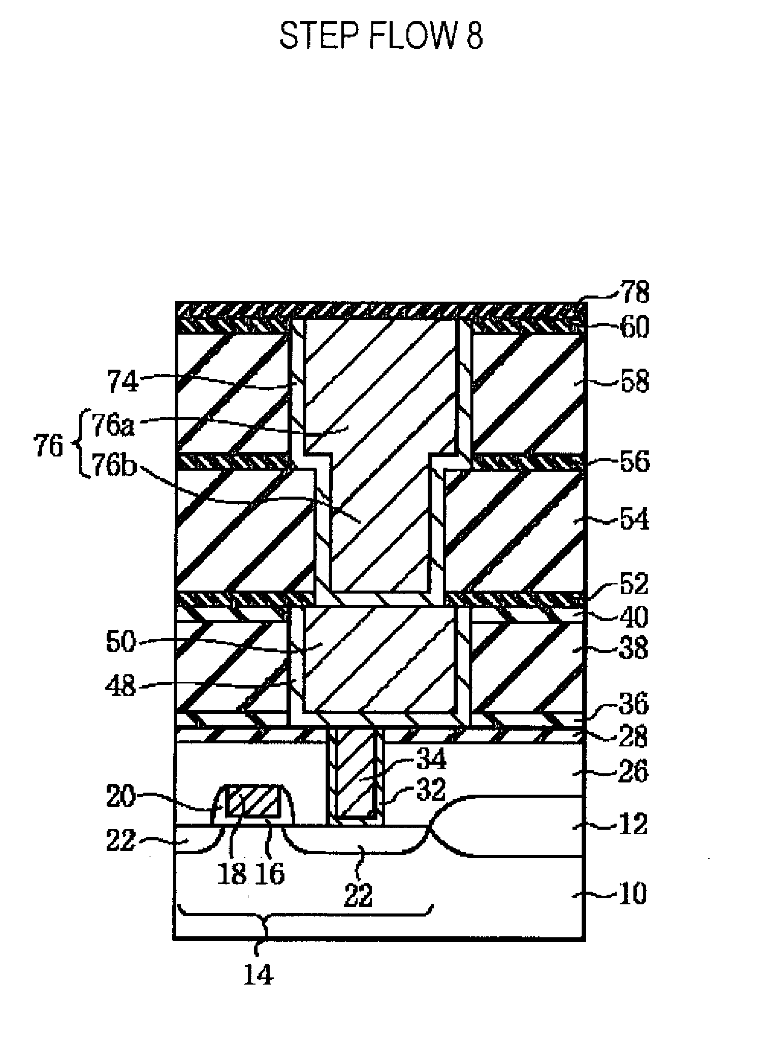
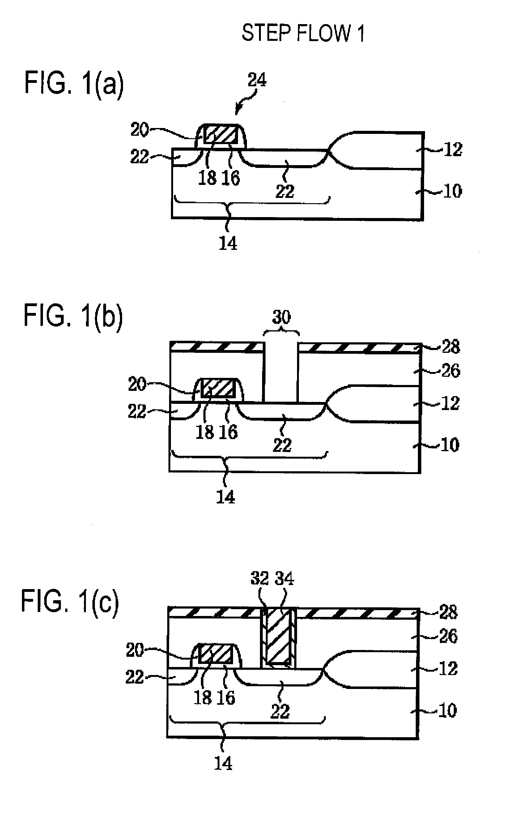
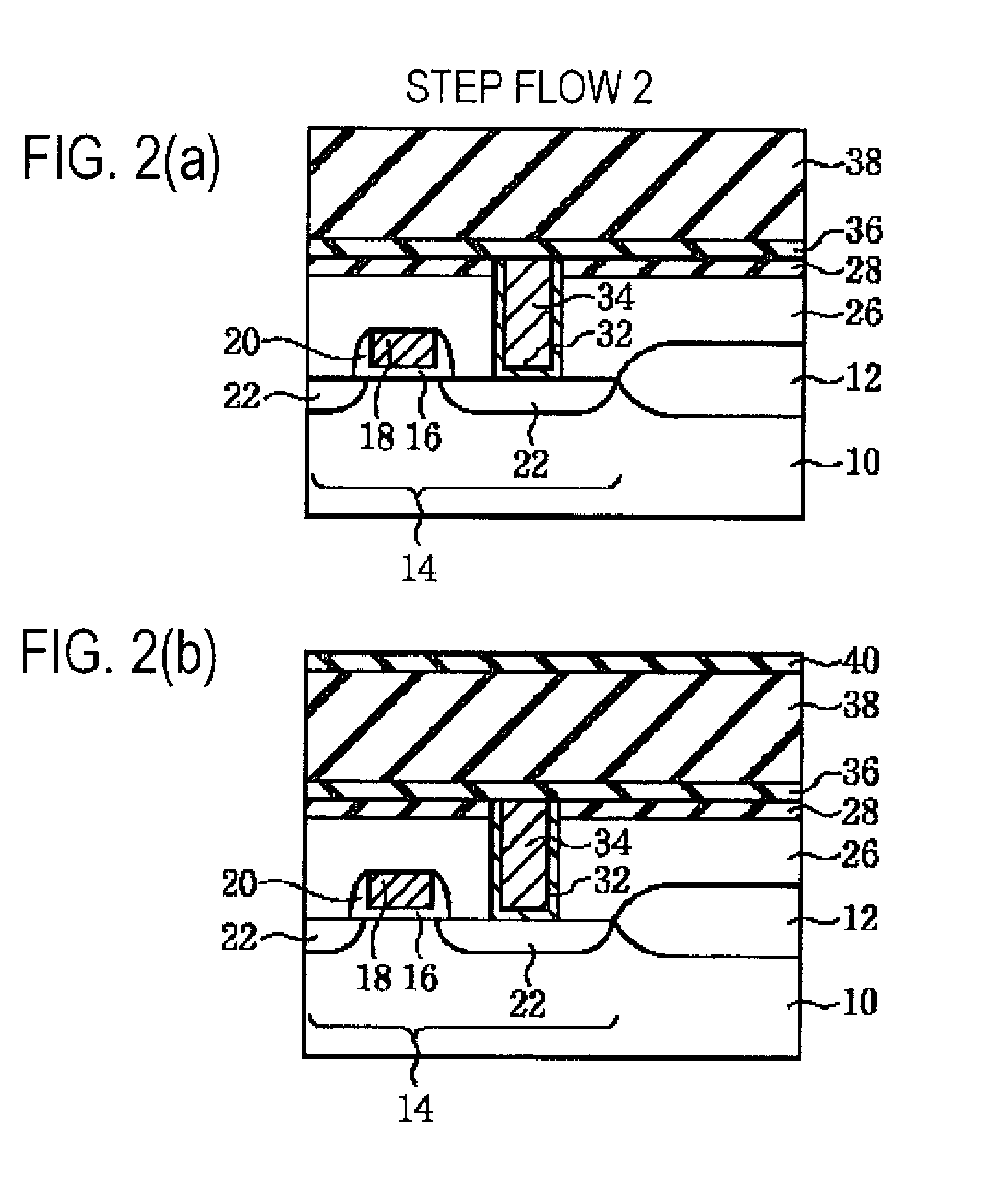
[0074] The following explanation will be made with reference to EXAMPLES 1-17 and COMPARATIVE EXAMPLES 1-6 of the present invention, as well as FIGS. 1-8. The curing with ultraviolet rays and evaluation were carried out as follows.

[0075] (Curing with Ultraviolet Rays)

[0076] A high-pressure mercury lamp (UVL-7000H4-N, Ushio electric Inc.) having a light-emission spectrum as shown in FIG. 11 was used for curing with ultraviolet rays. The illumination intensity and spectral distribution of ultraviolet rays were measured with a spectroradiometric illumination meter (USR-40D, Ushio electric Inc.).

[0077] (Ultraviolet Ray Spectrum)

[0078] The ultraviolet ray spectrum of an insulator film as shown in FIG. 9 was determined by measuring the ultraviolet ray spectrum of the insulator film in the range of 180-350 nm with a vacuum ultraviolet spectrometer (SGV-157, Shimadzu Corporation), the film having been formed on a quartz substrate.

[0079] (Specific Dielectric Constant)

[0080] A gold elec...


PUM


Abstract

In a method for manufacturing a semiconductor device, including forming an insulator film including a material having Si—CH3 bond and Si—OH bond, and irradiating the insulator film with ultraviolet rays, the rate of decrease of C concentration by X-ray photoelectron spectroscopy is not more than 30%, and the rate of decrease of one or more bonds selected from the group consisting of C—H bond, O—H bond and Si—O bond of Si—OH is not less than 10%, as a result of ultraviolet ray irradiation. A low-dielectric-constant insulator film that has a high film strength and can prevent increase of dielectric constant due to moisture absorption, a semiconductor device that can prevent device response speed delay and reliability decrease due to parasite capacity increase, and a manufacturing method therefor are provided.

Description

CROSS-REFERENCE TO RELATED APPLICATIONS [0001] This application is based upon and claims the benefit of priority from the prior Japanese Patent Application No. 2006-224236, filed on Aug. 21, 2006 and the prior Japanese Patent Application No. 2007-176433, filed on Jul. 4, 2007, the entire contents of which are incorporated herein by reference. BACKGROUND OF THE INVENTION [0002] 1. Field of the Invention [0003] The present invention relates to a multilayer wiring device and an insulator film thereof. [0004] 2. Description of the Related Art [0005] A drop in the signal propagation speed by the increase of parasitic capacity of an insulator film for a semiconductor device has been known, but the line delay did not have a major influence on an entire device at the generation in which the line space of a semiconductor device exceeded 1 μm. But the influence on the device speed becomes major when the line space is 1 μm or less, and in particular the influence of the parasitic capacity betw...

Claims


Application Information

Patent Timeline
Patent Type & Authority Applications(United States)
IPC IPC(8): H01L21/31
CPCH01L21/02126H01L21/02203H01L21/02348H01L21/76825H01L21/31695H01L21/76807H01L21/7682H01L21/3105H01L21/02216H01L21/31H01L21/3205
Inventor OZAKI, SHIROUNAKATA, YOSHIHIROYANO, EI
Owner FUJITSU LTD
Learn More