Silicon photovoltaic cell junction formed from thin film doping source

a technology of photovoltaic cells and junctions, applied in the direction of coatings, chemical vapor deposition coatings, plasma techniques, etc., can solve the problems of difficult gas source handling, affecting the performance and lifetime of the final pv system, and prior junction formation techniques are not economical for solar cell fabrication

Inactive Publication Date: 2008-03-06
APPLIED MATERIALS INC
View PDF21 Cites 49 Cited by
  • Summary
  • Abstract
  • Description
  • Claims
  • Application Information

AI Technical Summary

Benefits of technology

[0016]In still another aspect, an apparatus for fabricating a solar cell p-n junction on a sheet includes a chamber body, a sheet processing region adapted to processing one or more sheets having p-type silicon material thereon, one or more gas sources adapted to deliver a mixture of precursors comprising a silicon-containing compound, and a phosphorus-containing compound into the she

Problems solved by technology

Protection of the active PV devices during module construction directly affects the performance and lifetime of the final PV systems.
Although phosphorus diffusion of the phosphorus doped n-type silicon material for solar junction formation could be created by the furnace-type diffusion/annealing proce

Method used


Image

  • Silicon photovoltaic cell junction formed from thin film doping source
  • Silicon photovoltaic cell junction formed from thin film doping source
  • Silicon photovoltaic cell junction formed from thin film doping source

Examples


examples

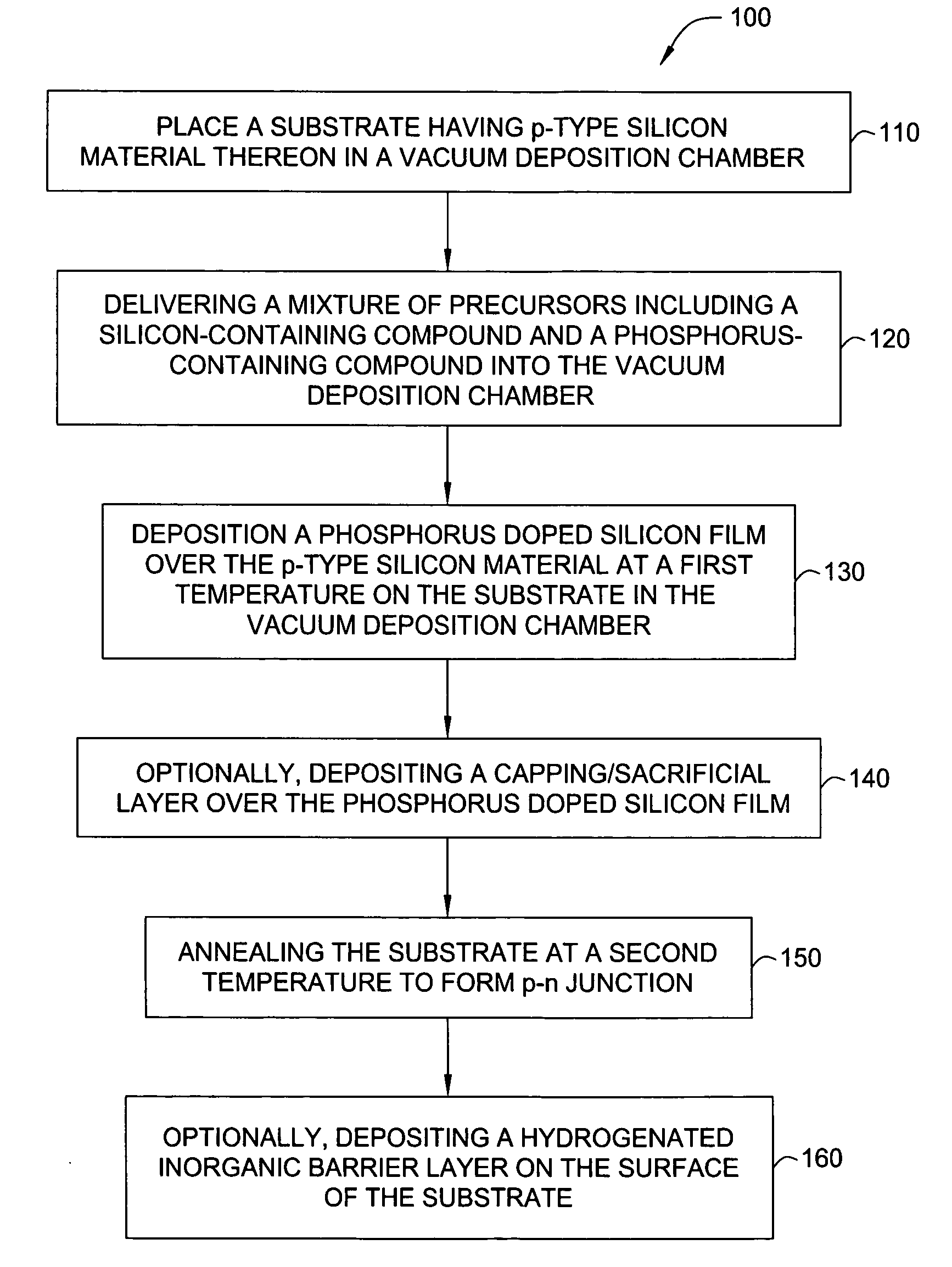
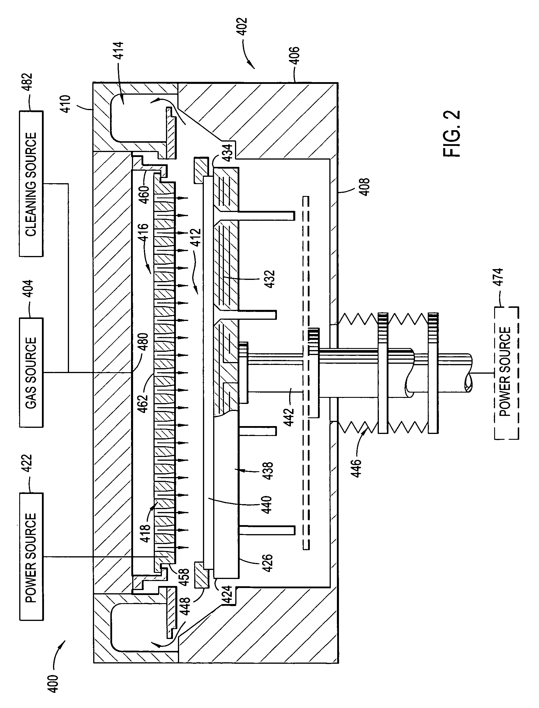
[0053]Sheets were brought under vacuum inside a plasma enhanced chemical vapor deposition (PECVD) system, available from Applied Materials, Inc., Santa Clara, Calif., with a spacing of about 900 mils to about 1000 mils. The temperature of the sheet support (susceptor) was set at about 350° C. for a low temperature deposition process.

[0054]Mixtures of silane (SiH4), phosphine (PH3), in the presence of hydrogen gas (H2) were delivered into the chamber as the source precursor gases for depositing a phosphorus-doped amorphous silicon film onto the sheet having p-type silicon material thereon. The pressure inside the chamber is about 0.7 Torr. A plasma was sustained with RF power generator set at about 13.56 MHz and about 250 W. The results showed that the deposited phosphorus doped amorphous silicon film exhibits good step coverage, good uniformity of about 10% or higher over the surface of the sheet (e.g., an uniformity of 70 nm to 90 nm at an average thickness of about 80 nm Å), and g...


PUM

PropertyMeasurementUnit
Percent by atomaaaaaaaaaa
Nanoscale particle sizeaaaaaaaaaa

Abstract

A method and apparatus for fabricating a solar cell and forming a p-n junction is disclosed. Solar cell p-n junction is formed by depositing a thin film of n-type phosphorus doped silicon material on a sheet from a mixture of precursors and annealing the sheet to obtain the p-n junction at a desired depth. In one embodiment, a plasma enhanced chemical vapor deposition chambers is used to deposit a phosphorus doped amorphous silicon film on a sheet surface by using precursors including a silicon-containing gas, a hydrogen-containing precursor, and a phosphorus-containing gas. In another embodiment, annealing furnace and/or rapid thermal processing chambers are used to anneal the sheet having the phosphorus doped amorphous silicon film deposited thereon.

Description

BACKGROUND OF THE INVENTION[0001]1. Field of the Invention[0002]Embodiments of the present invention generally relate to photovoltaic / solar cell and solar panel manufacturing.[0003]2. Description of the Related Art[0004]Photovoltaics (PV) systems can generate power for many uses, such as remote terrestrial applications, battery charging for navigational aids, telecommunication equipments, and consumer electronic devices, such as calculators, watches, radios, etc. One example of PV systems includes a stand-alone system which in general powers for direct use or with local storage. Another type of PV system is connected to conventional utility grid with the appropriate power conversion equipment to produce alternating current (AC) compatible with any conventional utility grid.[0005]PV or solar cells are material junction devices which convert sunlight into direct current (DC) electrical power. When exposed to sunlight (consisting of energy from photons), the electric field of solar cel...

Claims


Application Information

Patent Timeline
IPC IPC(8): H05H1/24C23C16/00
CPCC23C16/56C23C16/24
Inventor BACHRACH, ROBERTWON, TAE KYUNG
Owner APPLIED MATERIALS INC
Why Eureka
Try Eureka