Gallium nitride high electron mobility transistor having inner field-plate for high power applications

Inactive Publication Date: 2008-03-27
KOREA ADVANCED INST OF SCI & TECH
View PDF3 Cites 118 Cited by
  • Summary
  • Abstract
  • Description
  • Claims
  • Application Information

AI Technical Summary

Benefits of technology

[0008]Accordingly, the present invention has been made keeping in mind the above problems occurring in the prior art, and an object of the present invention is to provide a gallium-nitride high electron mobility transistor, in which an inner field-plate is disposed between the gate and drain of the high electron mobility transistor, so that an electric field is distributed between gate and drain regions to reduce a peak value and to reduce gate leak

Problems solved by technology

However, there are problems in that an electric field is not sufficiently distributed between the gate and drain regions of the high electron mobility transistor so that the electric field can be applied to microwaves, and in that the increment of a peak value relative to the electric field reduces the breakdown voltage.
Further, t

Method used


Image

  • Gallium nitride high electron mobility transistor having inner field-plate for high power applications
  • Gallium nitride high electron mobility transistor having inner field-plate for high power applications
  • Gallium nitride high electron mobility transistor having inner field-plate for high power applications

Examples


Embodiment Construction

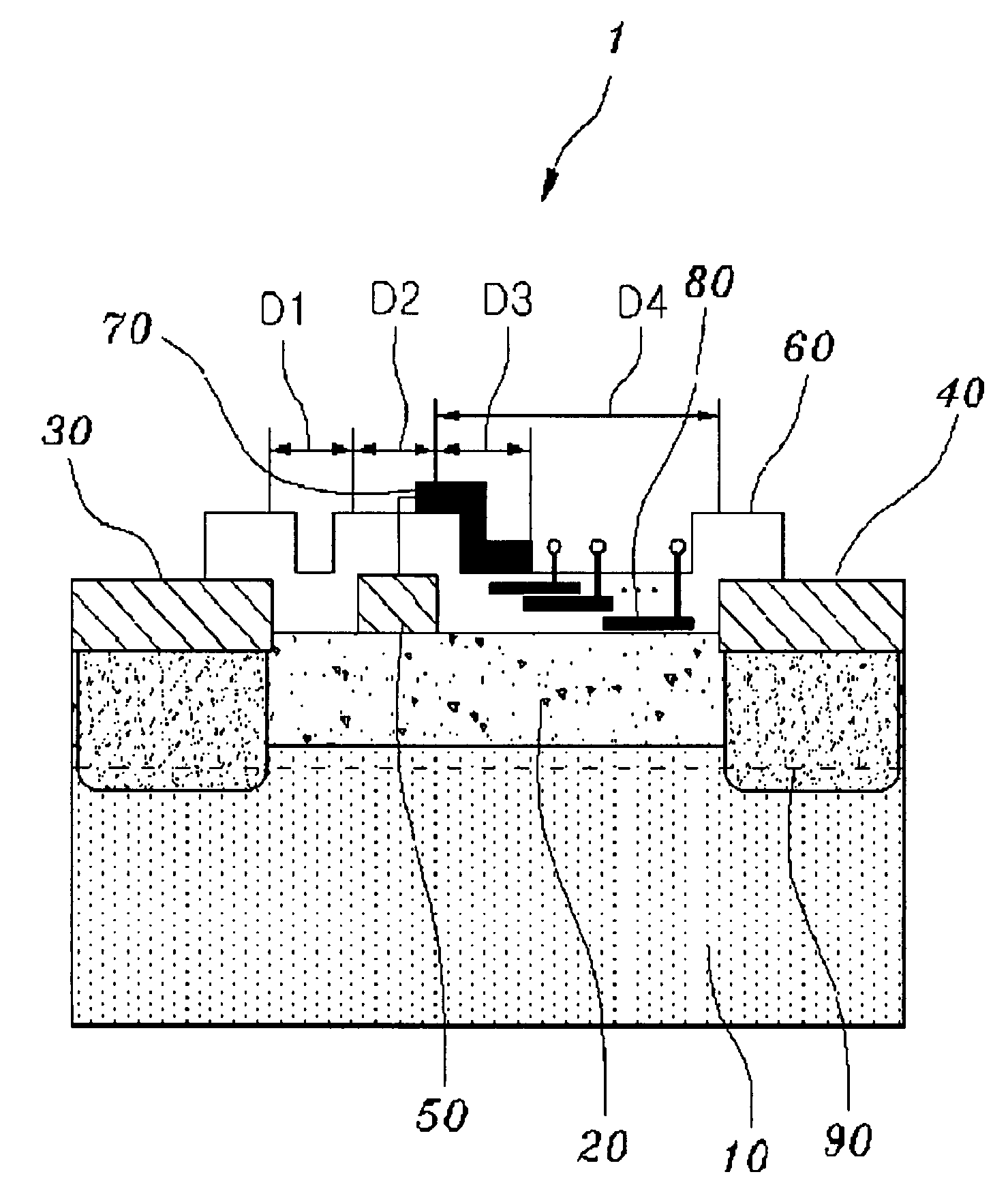
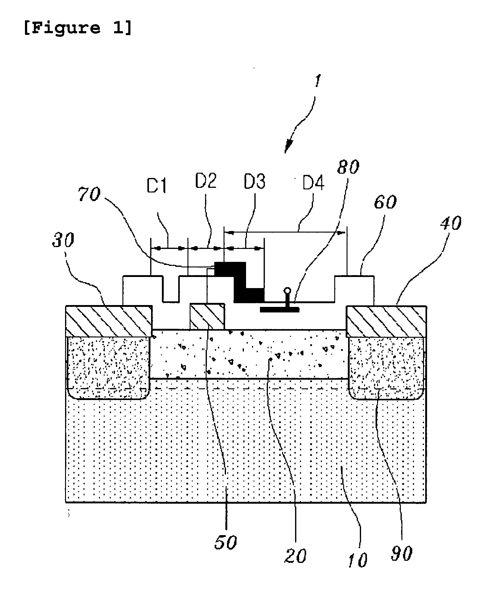
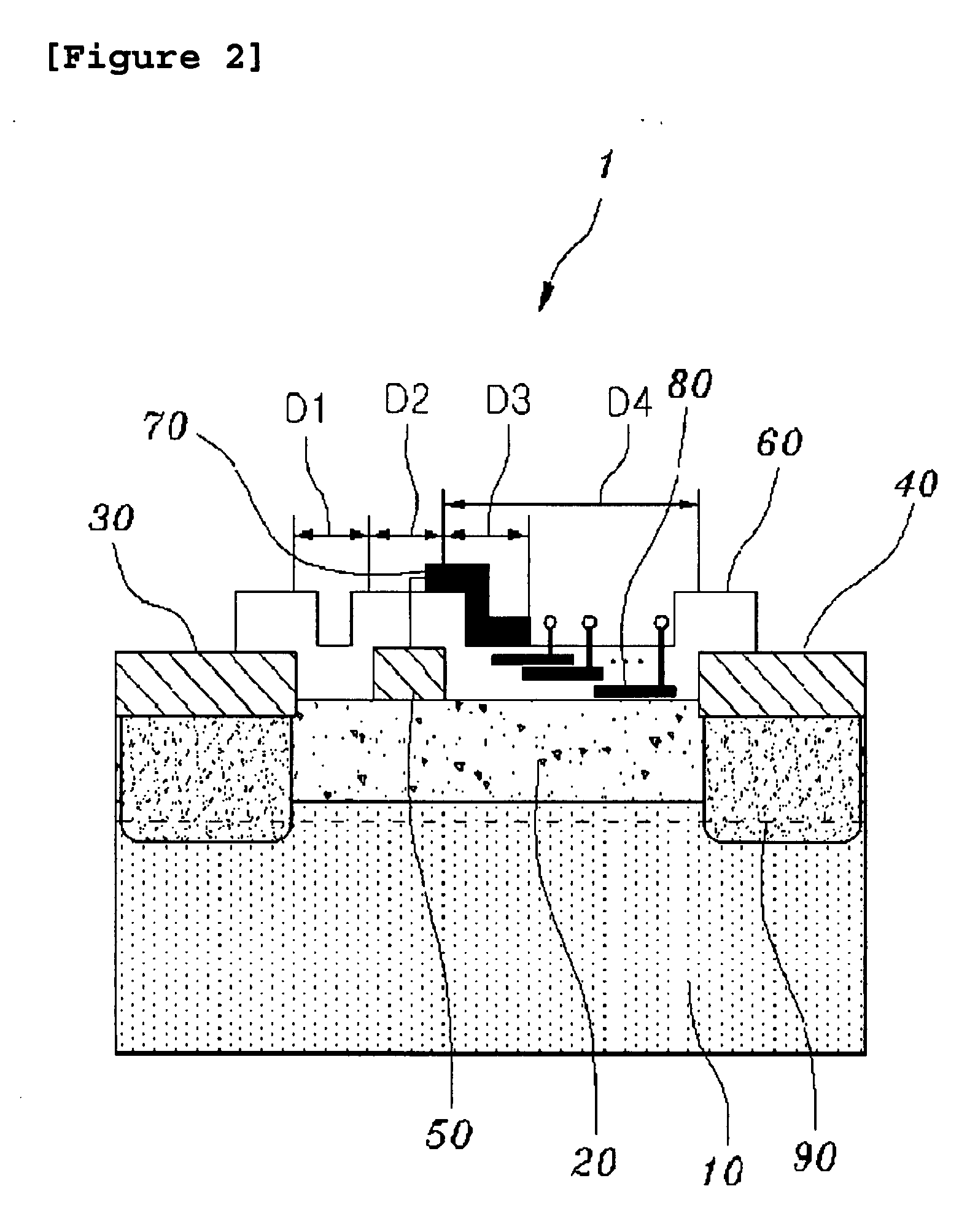
[0027]Hereinafter, embodiments of the present invention will be described in detail with reference to the attached drawings.

[0028]FIG. 1 is a sectional view schematically showing a High Electron Mobility Transistor (HEMT) according to the present invention, and FIG. 2 is a sectional view schematically showing an HEMT according to an embodiment of the present invention. As shown in the drawings, an HEMT 1 is constructed so that a gallium nitride (GaN) buffer layer 10, doped with Fe through Metal Organic Chemical Vapor Deposition (MOCVD), is formed, and a barrier layer 20 is formed on the buffer layer 10.

[0029]The buffer layer 10 is preferably made of a semi-conducting material and has a thickness of 2 μm, and the barrier layer 20 is preferably made of undoped Al0.27Ga0.73N and has a thickness of 22 nm. To isolate the devices, Remote Ion Beam Etching (RIBE), using Ar-Cl2 gas which has an etch rate of 400 Å / min, is preferably applied to the gallium nitride (GaN) buffer layer 10.

[0030]F...


PUM


Abstract

A gallium nitride high electron mobility transistor, in which an inner field-plate is disposed between the gate and drain of the high electron mobility transistor, so that an electric field is distributed between gate and drain regions to reduce a peak value and to reduce gate leakage current while maintaining high frequency performance, thus obtaining a high breakdown voltage, reducing the capacitance between the gate and the drain attributable to a shielding effect, and improving linearity and high power and high frequency characteristics through variation in the input voltage of the inner field-plate. The gallium-nitride high electron mobility transistor includes a gallium nitride buffer layer. An aluminum gallium-nitride barrier layer is formed on the buffer layer. A source electrode is placed on the barrier layer. A drain electrode is placed on the barrier layer to be spaced apart from the source electrode. A gate electrode is placed on a top of the barrier layer to be spaced apart from the source electrode and the drain electrode. A dielectric layer is deposited on the top of the barrier layer. An electric field electrode is formed on the dielectric layer located on the gate electrode. An inner field-plate is formed in the dielectric layer to be spaced apart from the gate electrode and the drain electrode.

Description

BACKGROUND OF THE INVENTION[0001]1. Field of the Invention[0002]The present invention relates, in general, to a gallium nitride high electron mobility transistor and, more particularly, to a gallium nitride high electron mobility transistor, in which an inner field-plate is disposed between the gate and drain of the high electron mobility transistor, so that an electric field is distributed between gate and drain regions to reduce a peak value and to reduce gate leakage current while maintaining high frequency performance, thus obtaining a high breakdown voltage, reducing capacitance between the gate and the drain attributable to a shielding effect, and improving linearity, and high power and high frequency characteristics through variation in the input voltage of the inner field-plate.[0003]2. Description of the Related Art[0004]Generally, a High Electron Mobility Transistor (HEMT) is applied to a high power and high integration transistor, a switch, a power amplifier, a Microwave ...

Claims


Application Information

Patent Timeline
IPC IPC(8): H01L29/739H01L31/00
CPCH01L29/2003H01L29/7787H01L29/404H01L29/7783
Inventor YANG, KYOUNGHOONLEE, SUNGSIKLEE, KIWONKO, KWANGUI
Owner KOREA ADVANCED INST OF SCI & TECH
Why Eureka
Try Eureka