

Organic light emitting display (OLED) and its method of manufacture
- Summary
- Abstract
- Description
- Claims
- Application Information
AI Technical Summary
Benefits of technology
Problems solved by technology
Method used
Image

Examples
embodiment 1
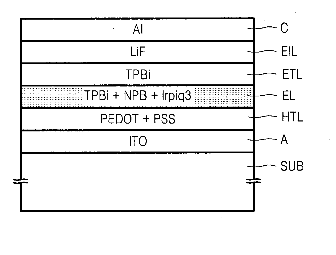
[0061]FIG. 1 is a cross-sectional view of an OLED and a method of manufacturing the OLED according to a first embodiment of the present invention.
[0062]Referring to FIG. 1, an anode A is formed on a substrate SUB. The anode A is formed of Indium Tin Oxide (ITO) serving as a first electrode. A Hole Transporting Layer (HTL) is formed on the anode A. The Hole Transporting Layer (HTL) is a composite layer made of PEDOT and PSS. The Hole Transporting Layer (HTL) is formed by baking a bare coating layer that includes PEDOT and PSS at a temperature of 180° C. for approximately one hour after the bare coating layer has been formed to a thickness of 50 nm. Next, a light emitting layer EL is formed on the Hole Transporting Layer (HTL). The light emitting layer EL includes a small molecule host and a light emitting dopant. The small molecule host includes at least an electron transporting host E-host and a hole transporting host H-host. The light emitting dopant is an organic molecule or organ...
embodiment 2
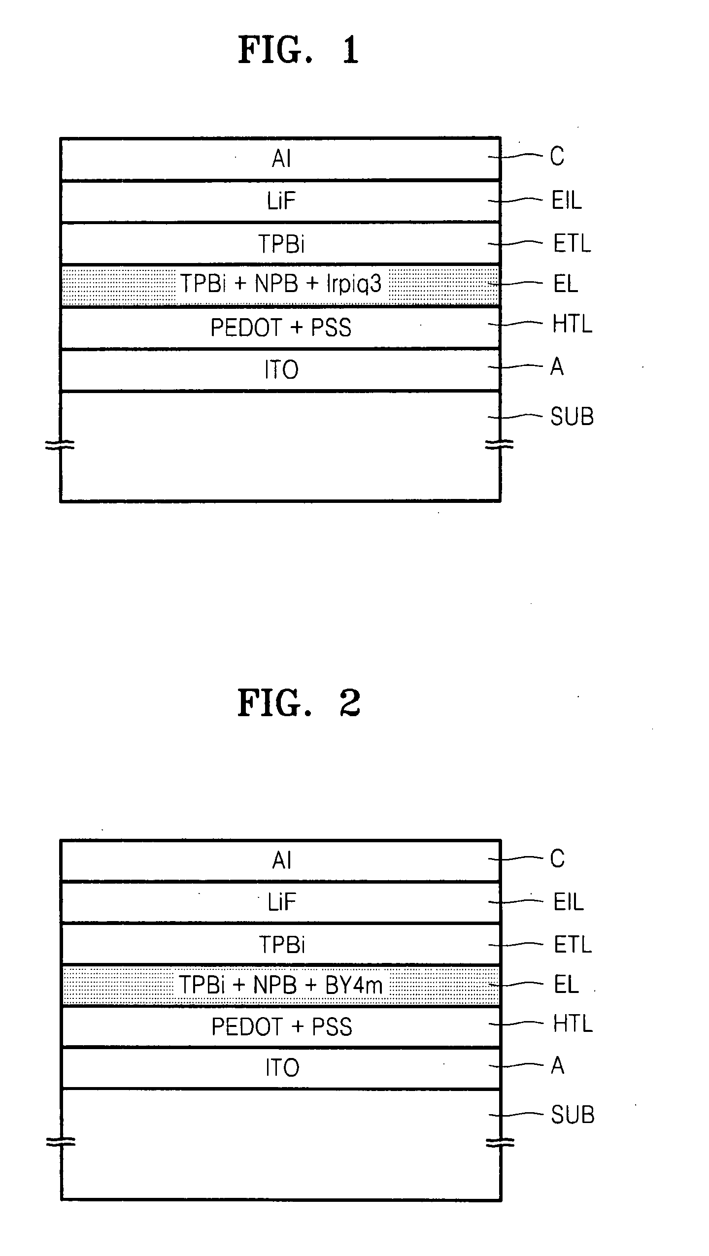
[0089]FIG. 2 is a cross-sectional view of an OLED and a method of manufacturing the OLED according to a second embodiment of the present invention.
[0090]Referring to FIG. 2, the second embodiment is the same as the first embodiment except that BY4m is used as a light emitting dopant.
embodiment 3
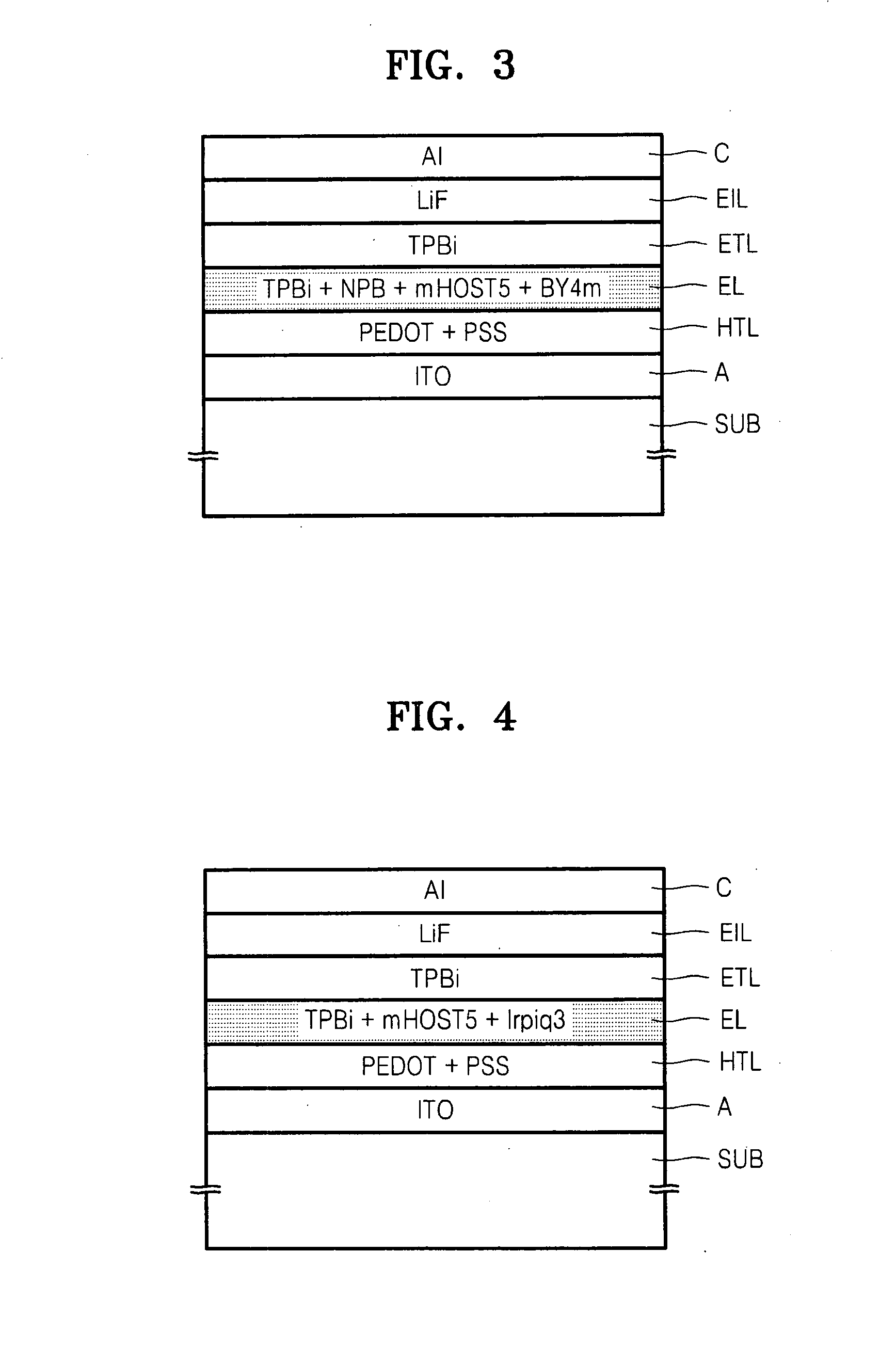
[0091]FIG. 3 is a cross-sectional view of an OLED and a method of manufacturing the OLED according to a third embodiment of the present invention.
[0092]Referring to FIG. 3, the third embodiment is the same as the first embodiment except that B1 in Table 2 is used as a small molecule host and BY4m is used as a light emitting dopant.
PUM
 Abstract
Description
Claims
Application Information