
Surface plasmon enhanced fluorescence sensor and fluorescence detecting method

a surface plasmon and fluorescence sensor technology, applied in the field of fluorescence sensors, can solve the problems of low fluorescence detection sensitivity, low sensitivity of fluorescence detection, and light scattered by impurities other than the detection target substance becomes noise, etc., to achieve high sensitivity, high excitation energy, and high sensitivity

Inactive Publication Date: 2008-03-27
FUJIFILM CORP
View PDF15 Cites 10 Cited by
  • Summary
  • Abstract
  • Description
  • Claims
  • Application Information

AI Technical Summary

Benefits of technology

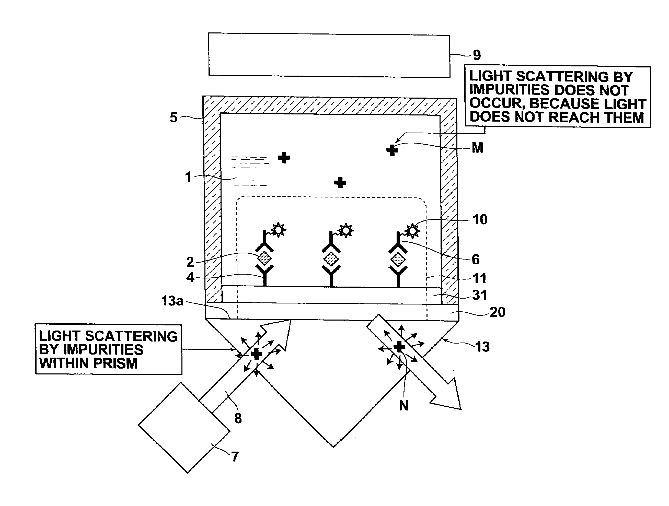
[0031]According to research performed by the present inventor, the reason why the sensitivity of fluorescence detection in the conventional surface plasmon enhanced fluorescence sensor provided with the SAM is not improved much is because the SAM is “spongy”. Therefore, the thickness of the SAM varies easily, which causes fluorescent substances within sample liquids to approach the metal film to distances where metallic light loss occurs.
[0050]The surface plasmon enhanced fluorescence sensor may be equipped with a kit that causes a labeled substance, which is an integrated substance constituted by the substance (such as the second messengers) that directly bonds with the capture molecules and a fluorescent substance excited by the evanescent waves, to be included within the sample. In this case, the kit can be used to easily introduce a labeled specific substance into the sample. Therefore, the aforementioned competitive fluorescence detection can be performed extremely easily.

Problems solved by technology

However, in conventional surface plasmon enhanced fluorescence sensors such as that illustrated in FIG. 3, the excitation light beam reflected or scattered at the interface between the substrate and the sample, and light scattered by impurities other than the detection target substance becomes noise.
Therefore, even if the performance of photodetectors is improved, the S / N ratio in fluorescence detection does not.
However, when fluorescence detection was performed using the aforementioned surface plasmon enhanced fluorescence sensor provided with the SAM, it was found that the sensitivity of fluorescence detection was not improved much, compared to a case in which the SAM is not provided.

Method used


Image

  • Surface plasmon enhanced fluorescence sensor and fluorescence detecting method
  • Surface plasmon enhanced fluorescence sensor and fluorescence detecting method
  • Surface plasmon enhanced fluorescence sensor and fluorescence detecting method

Examples


first embodiment

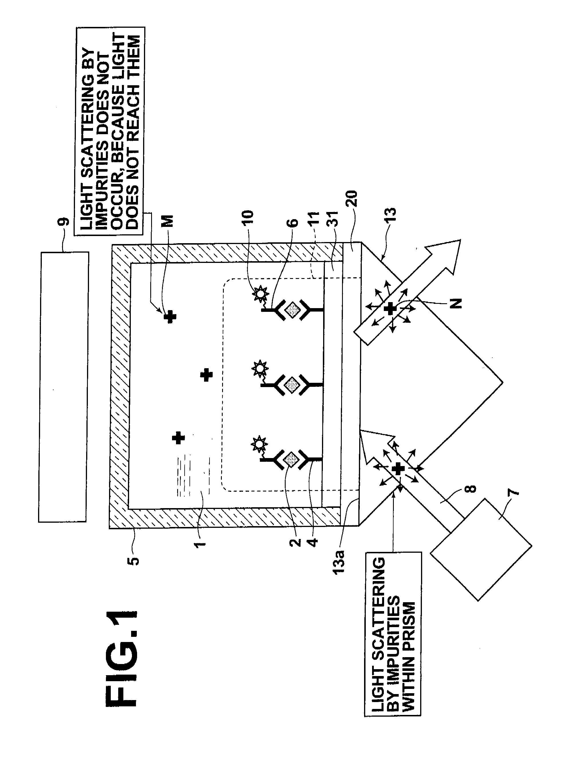
[0060]FIG. 1 is a side view that illustrates the schematic structure of a surface plasmon enhanced fluorescence sensor (hereinafter, simply referred to as “fluorescencesensor”) according to the present invention. As illustrated in FIG. 1, the fluorescence sensor comprises: a semiconductor laser light source 7, for emitting an excitation light beam 8 having a wavelength of 635 nm, for example; a prism 13 (dielectric block), formed of a material that transmits the excitation light beam 8 and provided at a position such that the excitation light beam 8 enters it at an end facet thereof; a metal film 20, formed on a surface 13a of the dielectric block 13; a non flexible polymer film, formed on the metal film 20; a sample holding portion 5, for holding a liquid sample 1 such that the liquid sample 1 contacts the non flexible polymer film 31 at the side opposite the prism 13; and photodetector 9 (fluorescence detecting means), provided above the sample holding portion 5.

[0061]Note that in...

second embodiment

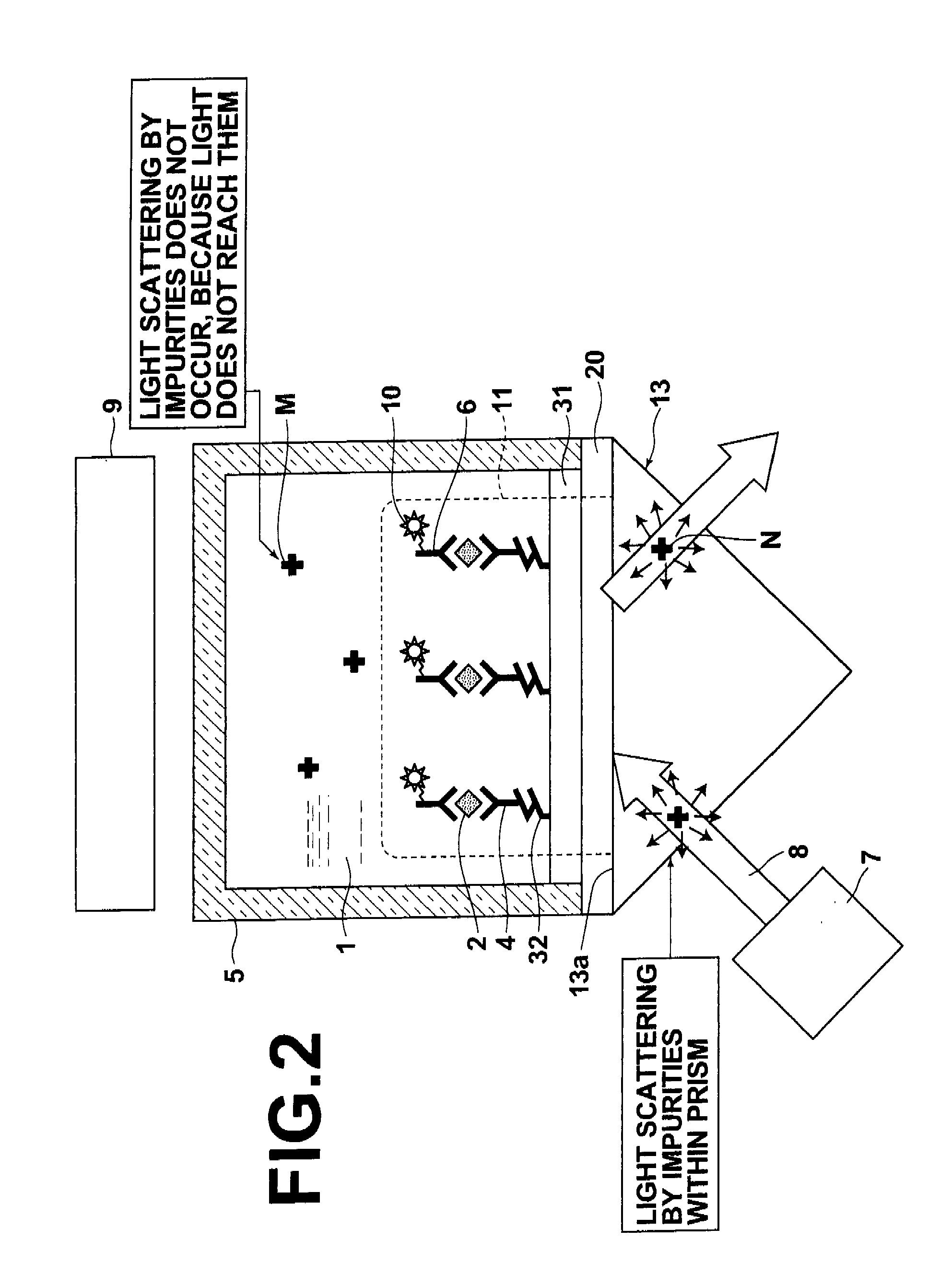
[0082]However, in the fluorescence sensor of the second embodiment, the linkers 32 that bond with the primary antibodies 4 are formed on the non flexible film 32. The linkers 32 block the secondary antibodies 6 and the antigens 2. Therefore, the secondary antibodies 6 and the antigens 2 are prevented from being non specifically adsorbed onto the non flexible film 31, and false positive detection is prevented. Meanwhile, the primary antibodies 4 which are to be provided on the surface of the non flexible film 31 may be specifically bonded with the linkers 32, to be supplied on the surface of the non flexible film 31.

[0083]Table 1 below compare and illustrate the detection limits of the fluorescence sensor of the second embodiment and conventional fluorescence sensors. In Table 1, the columns indicated by A, B, C, and D represent the detection limit of a conventional sensor having a basic structure as illustrated in FIG. 3, a conventional sensor that employs the ELISA method, a conven...


PUM

PropertyMeasurementUnit
thicknessaaaaaaaaaa
thicknessaaaaaaaaaa
thicknessaaaaaaaaaa

Abstract

A fluorescence sensor is constituted by: a light source, for emitting excitation light of a predetermined wavelength; a dielectric block, formed of a material that transmits the excitation light; a metal film, formed on a surface of the dielectric block; a non flexible film of a hydrophobic material, formed on the metal film at a film thickness within a range of 10 to 100 nm; a sample holding portion, for holding a sample such that the sample contacts the non flexible film; an incident optical system, for causing the excitation light to enter the interface between the dielectric block and the metal film through the dielectric block such that conditions for total internal reflection are satisfied; and fluorescence detecting means, for detecting fluorescence emitted by a substance within the sample, which is excited by evanescent waves that leak from the interface when the excitation light enters the interface.

Description

BACKGROUND OF THE INVENTION[0001]1. Field of the Invention[0002]The present invention relates to a fluorescence sensor that detects specific substances within samples by fluorometry. More specifically, the present invention relates to a fluorescence sensor that performs surface plasmon enhancement.[0003]2. Description of the Related Art[0004]Fluorometry is conventionally used in for biological measurements and the like, as an easy and highly sensitive measuring method. In fluorometry, a sample, which is considered to contain a detection target substance that emits fluorescence when excited by light having a specific wavelength, is irradiated with an excitation light beam of the aforementioned specific wavelength. The presence of the detection target substance can be confirmed by detecting the fluorescence due to the excitation. In the case that the detection target substance is not a fluorescent substance, a substance labeled by a fluorescent substance that specifically bonds with t...

Claims


Application Information

Patent Timeline
Patent Type & Authority Applications(United States)
IPC IPC(8): G01N21/55B82Y15/00G01N21/64G01N21/78G01N33/543G01N33/545G01N33/547
CPCG01N21/648G01N21/6428
Inventor OHTSUKA, HISASHIIKEDA, MORIHITO
Owner FUJIFILM CORP
Learn More