Method for forming strained silicon nitride films and a device containing such films

Active Publication Date: 2008-04-03
TOKYO ELECTRON LTD
View PDF5 Cites 72 Cited by
  • Summary
  • Abstract
  • Description
  • Claims
  • Application Information

AI Technical Summary

Benefits of technology

[0006]Thus, one aspect of the invention is to reduce or eliminate one or more of the

Problems solved by technology

First, post processing of the deposited film increases production steps thereby reducing throughput, and may require expensive special purpose tooling.
In addition, post processing of the deposited film primarily affects the film surface, which limits control of the str

Method used


Image

  • Method for forming strained silicon nitride films and a device containing such films
  • Method for forming strained silicon nitride films and a device containing such films
  • Method for forming strained silicon nitride films and a device containing such films

Examples


Example

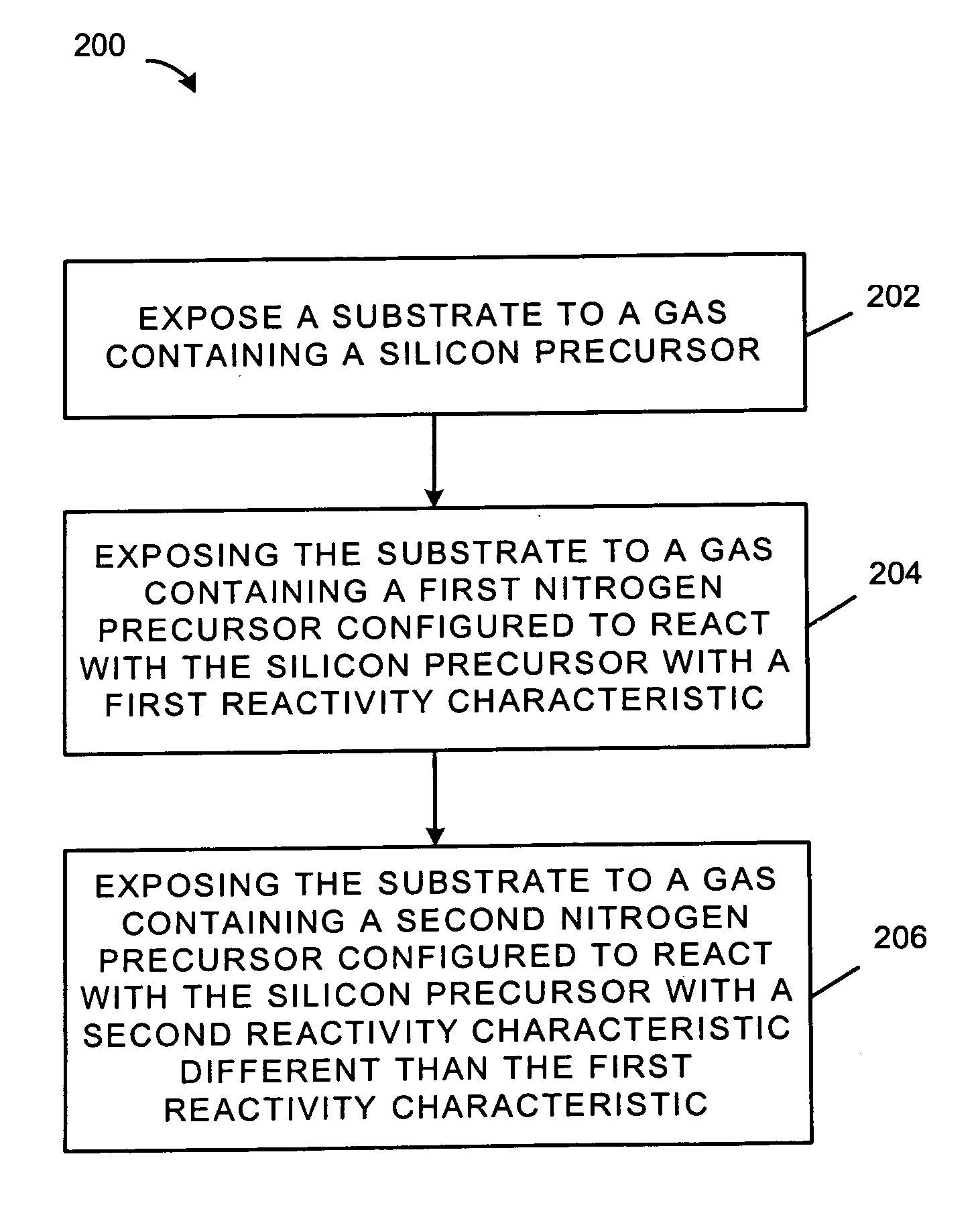
[0016]Embodiments of the invention describe processing methods to deposit strained SiN films utilizing a silicon precursor and different nitrogen precursors with different reactivity characteristics towards the silicon precursor. This difference in reactivity is at least in part due to the large difference in heat of formation (AH) of the different nitrogen precursors. Ammonia (NH3, ΔH=−45.9 kJ / mol) and hydrazine (N2H4, ΔH=95.35 kJ / mol) are examples of nitrogen precursors with a large difference in heat of formation.

[0017]According to embodiments of the invention, the difference in reactivity of the different nitrogen precursors towards a silicon precursor is utilized to deposit SiN films having a density gradient across the film thickness. For example, using the same or similar processing conditions, a first SiN film deposited using hydrazine can have a different deposition rate and different film density than a second SiN film deposited using ammonia. In some cases this difference...


PUM

PropertyMeasurementUnit
Ratioaaaaaaaaaa
Reactivityaaaaaaaaaa

Abstract

A method for forming a strained SiN film and a semiconductor device containing the strained SiN film. The method includes exposing the substrate to a gas including a silicon precursor. The substrate is exposed to a gas including a first nitrogen precursor configured to react with the silicon precursor with a first reactivity characteristic. The substrate is also exposed to a gas including a second nitrogen precursor configured to react with the silicon precursor with a second reactivity characteristic different than the first reactivity characteristic such that a property of the SiN film formed on the substrate changes to provide a strained SiN film. According to another embodiment, the substrate is exposed to a gas pulse containing a silicon precursor and first and second nitrogen precursors, wherein the ratio of the first and second precursors is varied during the exposure.

Description

FIELD OF THE INVENTION[0001]The present invention relates to semiconductor processing methods of forming strained silicon nitride films and semiconductor devices containing the strained silicon nitride (SiN) films.BACKGROUND OF THE INVENTION[0002]Nitride-based films are widely used in semiconductor devices and ultra-large-scale integrated circuits. For example, nitride films have been widely used in semiconductor devices as a diffusion barrier for dopants, as an etch-stop film during etching of fine features and as a final passivation film for encapsulation of fabricated devices, among many other uses. Nitride films can be deposited at low pressure or at atmospheric pressure using a variety of processing systems and process gases. These processing systems can perform, for example, thermal chemical vapor deposition (TCVD), plasma-enhanced chemical vapor deposition (PECVD), or remote-PECVD.[0003]Recent innovations to improve complementary metal oxide semiconductor (CMOS) transistor pe...

Claims


Application Information

Patent Timeline
IPC IPC(8): H01L21/44
CPCC23C16/345C23C16/45527H01L29/7843H01L21/76829H01L21/3185H01L21/0228H01L21/02211H01L21/0217
Inventor CLARK, ROBERT D.
Owner TOKYO ELECTRON LTD
Why Eureka
Try Eureka