Package structure and packaging method of MEMS microphone

Active Publication Date: 2008-04-10
IND TECH RES INST
View PDF7 Cites 58 Cited by
  • Summary
  • Abstract
  • Description
  • Claims
  • Application Information

AI Technical Summary

Benefits of technology

[0025] According to an embodiment of the present invention, a plurality of acoustic wave covers is fixed onto a plurality of MEMS microphone chips in a single step, and each component can be processed at the same time, thus the step of individually assembling the single housings may be avoided and thereby effectively increase the throughput.
[0026] According to an embodiment of the present invention, a mature molding process such as resin transfer molding can be used to package and protect a whole batch of MEMS

Problems solved by technology

Therefore, the market scale of mobile phone application cannot be ignored.
Similarly, based on the above reasons, the dispensing protection cannot be used for the MEMS microphone chip.
Also, in the current technique, the MEMS microphone chip is disposed in the acoustic wave cavity space, and is not protected by the molding compound, thus resulting in the following disadvantages.
(1) If the MEMS microphone module

Method used


Image

  • Package structure and packaging method of MEMS microphone
  • Package structure and packaging method of MEMS microphone
  • Package structure and packaging method of MEMS microphone

Examples


first embodiment

The First Embodiment

[0039] Referring to FIGS. 5-14, a method of packaging the MEMS microphone according to the first embodiment of the present invention is described.

[0040] Referring to FIGS. 5 and 17, FIG. 17 is a schematic plan view of the wafer, and FIG. 5 is a side sectional view of FIG. 17.

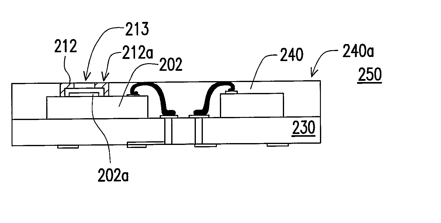
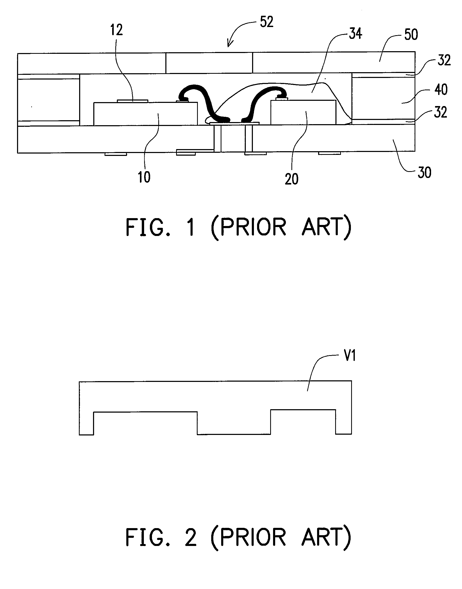
[0041] A wafer 200 is provided. The surface of the wafer 200 comprises a plurality of MEMS microphone chips 202. Each of the MEMS microphone chips 202 comprises at least a bonding pad 203, as shown in FIG. 5. One bonding pad 203 and an acoustic wave sensing portion 202a for sensing the acoustic wave is shown for each MEMS microphone chip 202 for the purpose of illustration.

[0042] Referring to FIG. 7, at least one acoustic wave cover 212 is provided, and the material of the acoustic wave cover 212 comprises but not limited to a conductive material, an ordinary radio-frequency-interference shielding material, an electromagnetic interference shielding material, or the like. The acoustic wave ...

second embodiment

The Second Embodiment

[0060] In the first embodiment, the MEMS microphone chip 202 and the logic chip 204 are disposed at the different positions of the substrate 230, for example, disposed parallel on the substrate 230. Referring to FIG. 15, in the second embodiment of the present invention, the MEMS microphone chip 202 is stacked on the logic chip 204. For example, the module unit 220 is stacked on the logic chip after the module unit 220 is obtained. In this embodiment, the electrical coupling of the MEMS microphone chip 202 and the substrate 230 is achieved by electrically coupling the bonding pad 203 of the MEMS microphone chip 202 to the bonding pad 233 of the logic chip 204, and then the connection pad 231 of the substrate is electrically coupled via the bonding pad 233 of the logic chip 204.

third embodiment

The Third Embodiment

[0061] In the second embodiment, the MEMS microphone chip 202 is stacked on the logic chip 204. Referring to FIG. 16, in the third embodiment of the present invention, the system chip 302 formed by integrating the MEMS microphone chip and the logic chip as whole can be adopted to replace the above stacking structure. The bonding pad 303 of the system chip 302 is directly wire-bonded to the connection pad 231 of the substrate.


PUM


Abstract

A package structure of a micro-electromechanical system (MEMS) type microphone is disclosed. The MEMS microphone comprises a substrate, a MEMS chip, an acoustic wave cover, and an encapsulant. The substrate has connection pads. The MEMS chip is electrically coupled to the connection pads. The MEMS chip includes an acoustic wave sensing portion. The acoustic wave cover is fixed on the MEMS chip for covering without contacting the acoustic wave sensing portion and defining an acoustic wave cavity space. The acoustic wave cover has an opening for allowing an acoustic wave to enter or exit out of the acoustic cavity space. The encapsulant encapsulates the substrate, the MEMS chip, and the acoustic wave cover, wherein a surface of the acoustic wave cover is exposed. The exposed surface of the acoustic wave cover is along the same level as the surface of the encapsulant.

Description

CROSS-REFERENCE TO RELATED APPLICATION [0001] This application claims the priority benefit of Taiwan application serial no. 95131712, filed Aug. 29, 2006. All disclosure of the Taiwan application is incorporated herein by reference. BACKGROUND OF THE INVENTION [0002] 1. Field of the Invention [0003] The present invention relates to a package structure and a packaging method of a micro-electromechanical (MEMS) microphone. [0004] 2. Description of Related Art [0005] Under the influence of the popular global communication, it is common that one person may have one or more mobile phones or everyone has a mobile phone. Even students carry mobile phones to school for communicating with parents, and thus the mobile phone consumer age is significantly lowered to below 10-year old. [0006] Further, the Topology Research Institute points out in the September 2005 research report that the global shipment quantity of the mobile phones in 2005 was about 760 million, and the number of mobile phone...

Claims


Application Information

Patent Timeline
IPC IPC(8): H01L29/84H01L21/56
CPCH04R1/04H01L2924/1461H04R19/005H01L2224/73265H01L2224/48465H01L2224/48227H01L2224/48091H01L2224/32225H01L24/97H01L2924/00014H01L2924/00H01L2924/15787H01L2224/97H01L2924/181
Inventor CHEN, JUNG-TAICHU, CHUN-HSUN
Owner IND TECH RES INST
Why Eureka
Try Eureka