Plasma display panel, a method for manufacturing a plasma display panel, and related technologies

a technology of plasma display panel and display panel, which is applied in the manufacture of electrode systems, electric discharge tubes/lamps, natural mineral layered products, etc., can solve the problems of limited realization of current cathode ray tubes (crts), increased restrictions on the material containing pb, and environmental pollution, so as to improve the cost-competitiveness of pdp and reduce the cost. , the effect of low curing temperatur

Inactive Publication Date: 2008-04-10
LG ELECTRONICS INC
View PDF2 Cites 3 Cited by
  • Summary
  • Abstract
  • Description
  • Claims
  • Application Information

AI Technical Summary

Benefits of technology

[0030]A dielectric composition for a PDP consistent with this disclosure may be free of Pb and the environmental pollution caused by Pb, largely improving cost-competitiveness of the PDP due to a relatively low unit cost, and ensuring a sufficiently low curing temperature such that thermal deformation on a substrate can be avoided in the manufacturing of the PDP.
[0031]A PDP including a dielectric layer made of a Pb-free dielectric composition consistent with this disclosure may largely improve cost-competitiveness of the PDP due to a relatively low unit cost, and ensure a sufficiently low curing temperature such that thermal deformation on a soda-lime glass substrate can be avoided in the manufacturing of the PDP. In addition, distortion between the substrate and the dielectric layer can be prevented by having a thermal expansion coefficient that matches the thermal expansion coefficient of the soda-lime glass substrate.
[0032]A PDP including barrier ribs formed using a dielectric composition consistent with this disclosure can be free from Pb and the environmental pollution caused by Pb, largely improving cost-competitiveness of the PDP due to a relatively low unit cost, and ensuring a sufficiently low curing temperature such that thermal deformation on a substrate can be avoided in the manufacturing of the PDP.
[0033]A PDP including a white dielectric layer formed using a dielectric composition consistent with this disclosure can be free from Pb and the environmental pollution caused by Pb, largely improving cost-competitiveness of the PDP due to a relatively low unit cost, and ensuring a sufficiently low curing temperature such that thermal deformation on a substrate can be avoided in the manufacturing of the PDP.

Problems solved by technology

However, current cathode ray tubes (CRTs) may be limited in realizing large screens of 40 inches or more.
However, given problems such as environmental pollution due to using Pb, restrictions on the material containing Pb are being intensified.
The Bi-based dielectric composition also causes environmental pollution, and unit cost of the composition is high.
However, since the Zn-based dielectric composition has a high glass transition temperature (Tg), the Zn-based dielectric composition does not meet with the curing conditions of the dielectric composition when using the soda-lime glass.
As a result, thermal deformation of the soda-lime glass occurs during curing due to such a high curing temperature.
Additionally, since the thermal expansion coefficient of the soda-lime glass is higher than the conventional PD-200 glass, distortion may occur due to the difference in the thermal expansion coefficient between the soda-lime glass and the dielectric layer, in consideration of the heat generation characteristic of the plasma display panel, unless the dielectric composition also has a high thermal expansion coefficient.

Method used


Image

  • Plasma display panel, a method for manufacturing a plasma display panel, and related technologies
  • Plasma display panel, a method for manufacturing a plasma display panel, and related technologies
  • Plasma display panel, a method for manufacturing a plasma display panel, and related technologies

Examples


Embodiment Construction

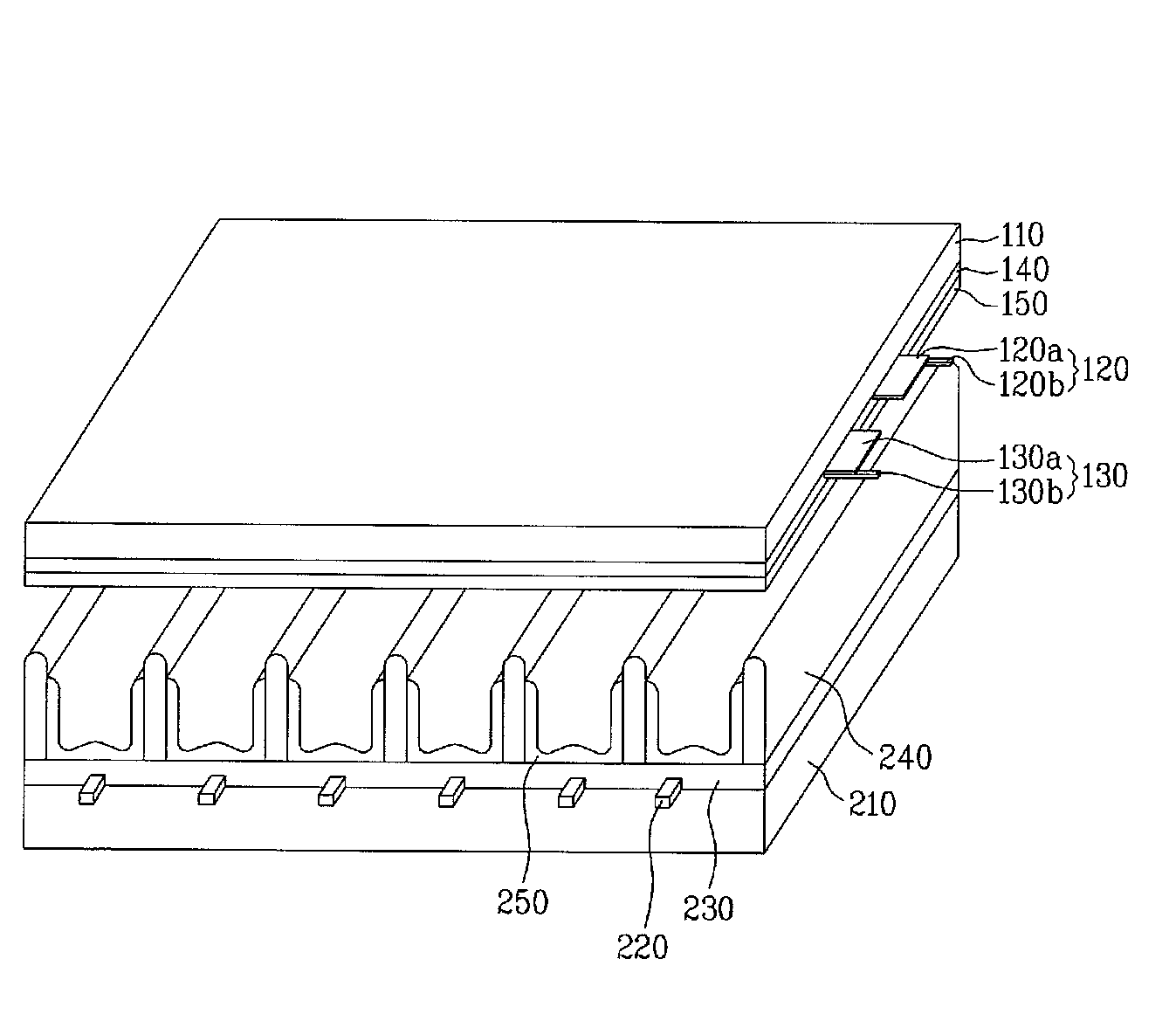
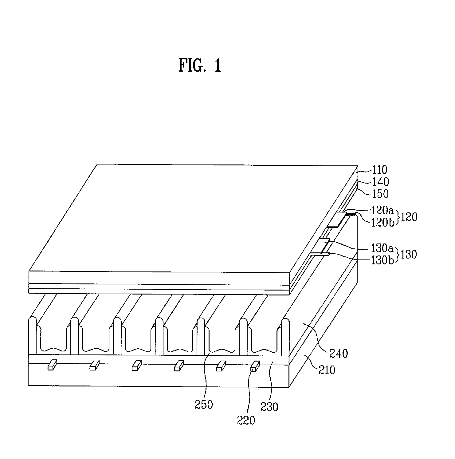
[0038]The thickness ratios of the layers shown in FIG. 1 and FIG. 2 are not actual thickness ratios. Furthermore, when an element such as a layer, film, region or substrate is referred to as being “on” another element, it can be directly on the other element or intervening elements may also be present (e.g., interposed between the elements).

[0039]As shown in FIG. 1, a PDP includes display electrodes 120 and 130 formed in pairs on the front substrate 110 while extending in one direction. A display electrode pair may include a scan electrode and a sustain electrode. Each display electrode 120 or 130 includes a transparent electrode 120a or 130a typically made of indium tin oxide (ITO), and a bus electrode 120b or 130b typically made of a metal material (e.g., silver, chromium, and / or copper). The PDP also includes a dielectric layer 140 and a protect layer 150. The layers 140 and 150 may be sequentially formed, in this order, over the overall surface of the front substrate 110, to cov...


PUM

PropertyMeasurementUnit
mol %aaaaaaaaaa
temperatureaaaaaaaaaa
particle sizeaaaaaaaaaa

Abstract

A plasma display panel includes a substrate with electrodes. A dielectric layer is disposed over the substrate and covers the electrodes. The dielectric layer includes 10 to 60 mol % of Bi2O3, 5 to 40% of CuO, and 15 to 40 mol % of B2O3.

Description

[0001]This application claims priority from Korean Patent Application No. 10-2006-0098326, filed Oct. 10, 2006, in the Korean Intellectual Property Office, the entirety of which is incorporated by reference herein.BACKGROUND[0002]1. Field[0003]This disclosure relates to a plasma display panel and a method for manufacturing the plasma display panel.[0004]2. Discussion of the Related Art[0005]The advent of the multimedia age has brought a demand for large display devices capable of finely rendering colors that approximate natural colors. However, current cathode ray tubes (CRTs) may be limited in realizing large screens of 40 inches or more. For this reason, liquid crystal displays (LCDs), plasma display panels (PDPs), and projection televisions (TVs) are being rapidly developed so that they can be used for high-quality images.[0006]A PDP is an electronic device that displays an image using a plasma discharge. By applying a predetermined voltage to electrodes arranged in a discharge s...

Claims


Application Information

Patent Timeline
Patent Type & Authority Applications(United States)
IPC IPC(8): B32B9/04B23P17/04
CPCC03C3/14C03C3/145C03C3/15Y10T29/49H01J11/12H01J11/38H01J9/02C03C3/12C03C3/23
Inventor KWON, TAE IN
Owner LG ELECTRONICS INC
Why Eureka
Try Eureka