
Method for measuring interface traps in thin gate oxide MOSFETs

Inactive Publication Date: 2008-04-24
TEXAS INSTR INC
View PDF8 Cites 15 Cited by
  • Summary
  • Abstract
  • Description
  • Claims
  • Application Information

AI Technical Summary

Problems solved by technology

Contaminants and other defects at the oxide silicon interface can cause problems in the manufacture and performance of integrated circuits that are fabricated over that interface.
Interface traps can have an adverse effect on device performance, for example, an interface trap can cause discrete switching in the source conductance, band-to-band tunneling (BBT) of hot carriers from the gate-to-drain which can result in gate-induced drain leakage current, drain current fluctuation, voltage drop in the gate area, threshold voltage shift in the MOS transistors, and the like.
The traditional charge pumping technique for characterizing interface traps fails when tunneling current is comparable to or greater than the charge pumping current, as it is difficult to separate the two currents.
A-priori estimation of the average gate tunneling current (which is a function of the gate voltage waveform) into the bulk or source / drain of the MOSFET during charge pumping leads to inaccuracies due to the exponential dependence of gate tunneling current on the gate voltage.
However, some of the traps will remain “trapped” and recombine with the inversion charge or the accumulation charge coming from the bulk.
There is a substantial current measurement difference between devices, when evaluating an enhanced complementary metal oxide semiconductor (CMOS) as opposed to a MOSFET where they gate dielectric is very thin.
Utilizing a thin gate dielectric, if there is an increase in the voltage beyond inversion, or if the device is taken to deep accumulation, that results in a significant amount of gate current.
However, this gate current is small, when compared to a normal MOSFET operating current, which is the source / drain current.

Method used


Image

  • Method for measuring interface traps in thin gate oxide MOSFETs
  • Method for measuring interface traps in thin gate oxide MOSFETs
  • Method for measuring interface traps in thin gate oxide MOSFETs

Examples


Embodiment Construction

[0023]The following description of the embodiment below is merely an example and is in no way intended to limit the invention or its application or uses. The present invention discloses a method for measuring interface traps in thin gate oxide MOSFET devices.

[0024]As semiconductor devices get smaller, hot carrier induced degradation of those devices is apt to occur. In order to make the MOSFET devices or Ultra-Large-Scale Integration (ULSI) components more reliable, it is critical to understand and quantify this degradation condition. The technique mentioned supra to accomplish this utilizes a charge pumping method, which is a measurement technique that can evaluate the substrate surface conditions at the Si—SiO2 interface, for example.

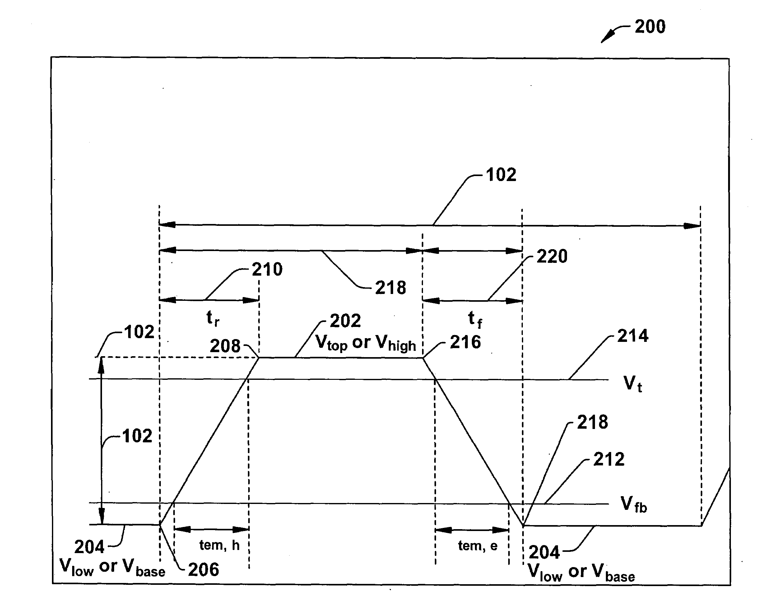
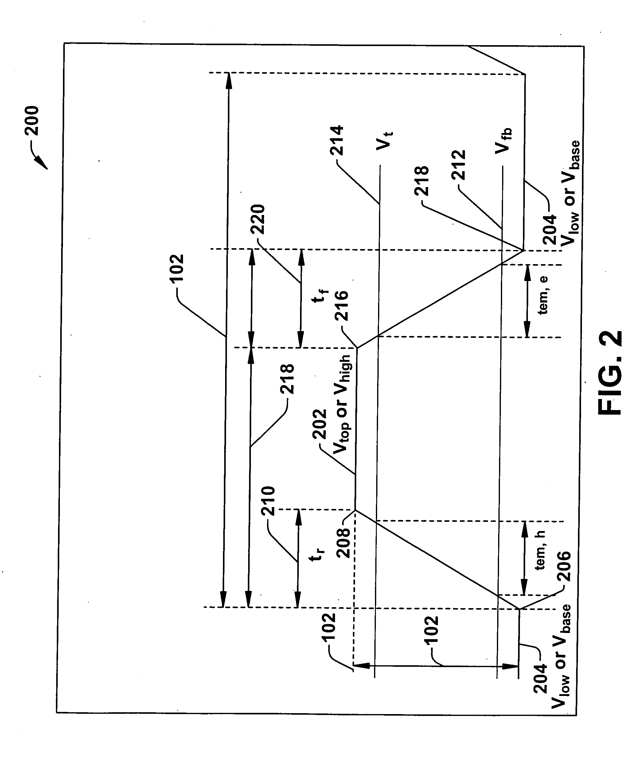
[0025]Turning now to the figures, FIG. 2 illustrates a trapezoidal wave pulse according to an aspect of the present invention. The interface traps between the Si and SiO2 layers that recombine with inversion or accumulation charges will constitute a n...


PUM


Abstract

A method for measuring interface traps in a MOSFET, comprising measuring charge pumping current of a pulse wave form for various frequencies over a predetermined frequency range, creating plotted points of the measured charge pumping current versus the predetermined frequency range, determining the total number of interface traps participating in the charge pumping current by calculating the slope of a best fit line through the plotted points.

Description

TECHNICAL FIELD[0001]The present invention relates to interface traps within MOSFETs, and in particular to a method for measuring interface traps in thin gate oxide MOSFETs.BACKGROUND OF THE INVENTION[0002]As is known in the art, semiconductor wafers often contain material interfaces such as between silicon and silicon dioxide. Contaminants and other defects at the oxide silicon interface can cause problems in the manufacture and performance of integrated circuits that are fabricated over that interface. These defects, often referred to as interface traps, are capable of trapping and de-trapping charge carriers. Interface traps can have an adverse effect on device performance, for example, an interface trap can cause discrete switching in the source conductance, band-to-band tunneling (BBT) of hot carriers from the gate-to-drain which can result in gate-induced drain leakage current, drain current fluctuation, voltage drop in the gate area, threshold voltage shift in the MOS transis...

Claims


Application Information

Patent Timeline
IPC IPC(8): G01R31/26
CPCG01R31/2621
Inventor CHATTERJEE, TATHAGATACHATTERJEE, AMITAVA
Owner TEXAS INSTR INC
Learn More