Interconnect structure of semiconductor integrated circuit, and design method and device therefor

a technology of integrated circuits and interconnects, applied in the field of interconnect structures of semiconductor integrated circuits, can solve the problems of increasing parasitic capacitance between interconnects, increasing power consumption, and increasing rc delay of interconnects, so as to suppress the reduction of parasitic capacitance, reduce the yield, and produce in a short time

Active Publication Date: 2008-04-24
PANASONIC SEMICON SOLUTIONS CO LTD
View PDF13 Cites 154 Cited by
  • Summary
  • Abstract
  • Description
  • Claims
  • Application Information

AI Technical Summary

Benefits of technology

[0037] According to the interconnect structure and the design method of the present invention, interconnects in which a detriment due to air gap-caused reduction in parasitic capacitance between interconnects has been minimized can be produced in a short tim

Problems solved by technology

Higher integration however extremely narrows the spacing between interconnects, causing a problem of increase in parasitic capacitance between interconnects.
The increase in parasitic capacitance between interconnects will result in occurrence of a crosstalk phenomenon in which an electric signal leaks between interconnects, increase of a RC delay of interconnects and increase of power consumption.
The open width of such voids has an upper limit for allowing generation of air gaps depending on the material of the insulating film.
However, the conventional ways of generating air gaps have the following problems.
First, no consideration has been given to a detriment that may result from imprudent reduction of the parasitic capacitance between interconnects.
In the under 180 nm process, hold timing errors occur frequently because of increase in the propagation time lag of a clock signal (clock skew) caused by crosstalk, IR drop,

Method used


Image

  • Interconnect structure of semiconductor integrated circuit, and design method and device therefor
  • Interconnect structure of semiconductor integrated circuit, and design method and device therefor
  • Interconnect structure of semiconductor integrated circuit, and design method and device therefor

Examples


embodiment 1

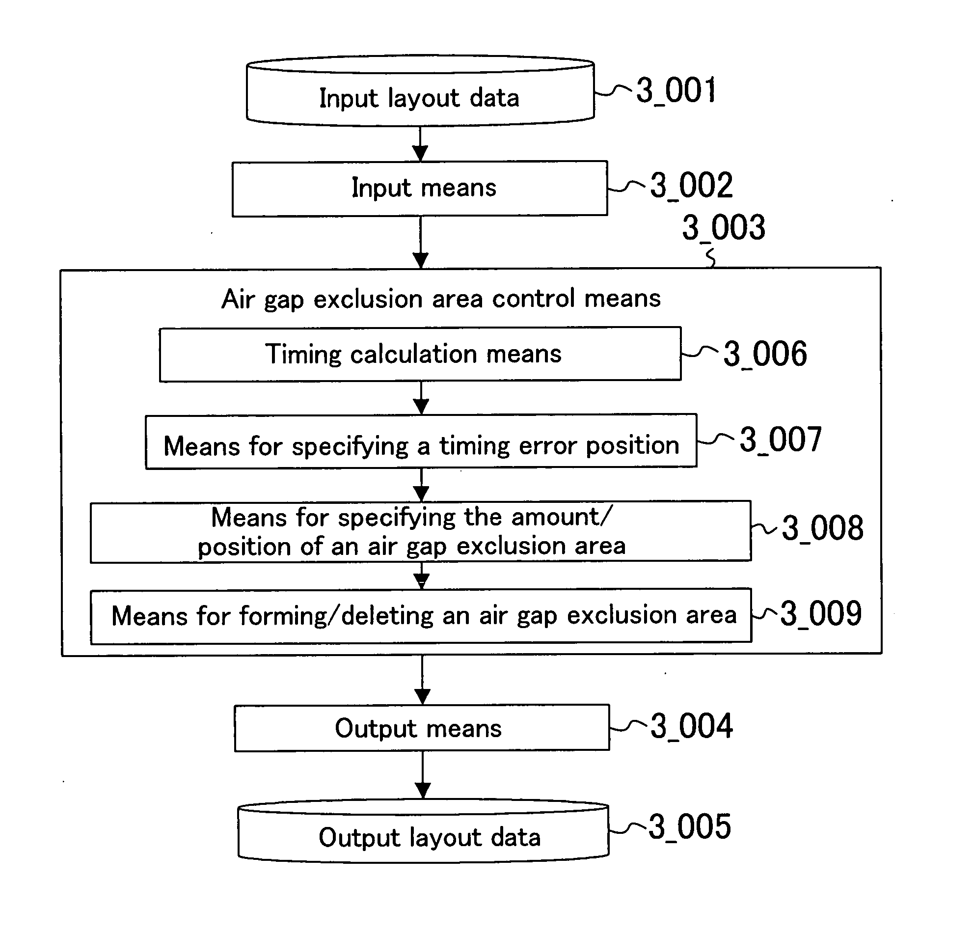
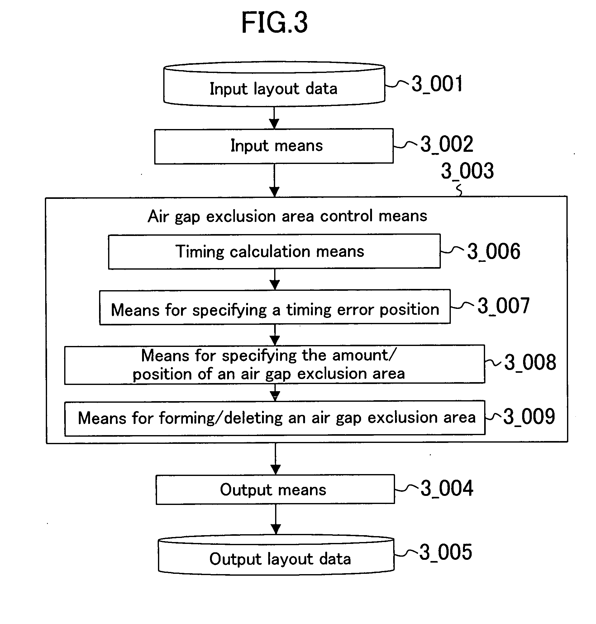
[0072]FIG. 3 is a block diagram of a design device for an interconnect structure in Embodiment 1 of the present invention. Referring to FIG. 3, the design device for an interconnect structure includes: an input means 3_002 for receiving input layout data 3_001; an air gap exclusion area control means 3_003 for controlling air gap exclusion areas based on interconnects in the input layout data; and an output means 3_004 for outputting output layout data 3_005 including information on determined air gap exclusion areas. The air gap exclusion area control means 3_003 includes: a timing calculation means 3_006; a means 3_007 for specifying a timing error position; a means 3_008 for specifying the amount / position of an air gap exclusion area; and a means 3_009 for forming / deleting an air gap exclusion area.

[0073] The air gap exclusion area control means 3_003 forms / deletes an air gap exclusion area in the air gap exclusion area control step 2 in FIG. 1 described above.

[0074]FIG. 4 is a...

embodiment 2

[0087] A design method for an interconnect in Embodiment 2 of the present invention will be described.

[0088] In the design technique for an interconnect structure shown in Embodiment 1, the influence of the air gap amount on timing is calculated in the step 4_003 of specifying the amount / insertion position of an air gap exclusion area. This causes a problem of increasing the processing time.

[0089] In this embodiment, in the step 4_003, no calculation of the air gap exclusion area amount is made, but the following measures are taken for a timing error position. That is, an air gap exclusion area is uniformly formed for a hold error position while an air gap exclusion area is uniformly deleted for a setup error position.

[0090] Referring to FIGS. 6A to 6C, an interconnect structure in this embodiment will be described.

[0091]FIG. 6A shows an interconnect 6_003 connecting a cell 6_001 with a cell 6_002. Assume that the interconnect 6_003 has been specified as having a hold timing err...

embodiment 3

[0097] A design method for an interconnect structure in Embodiment 3 of the present invention will be described.

[0098] In the design methods for an interconnect structure shown in Embodiments 1 and 2, timing is calculated, and after specifying a timing error position, an air gap exclusion area is formed to avoid a timing error. For timing calculation, it is necessary to perform complicate delay calculation, and this disadvantageously requires a huge amount of calculation time.

[0099] This embodiment is characterized in forming air gap exclusion areas based on the total interconnect length of a path without calculating timing.

[0100]FIG. 7 is a flowchart showing the design method for an interconnect structure in this embodiment related to the air gap exclusion area control step 2 in FIG. 1 described above.

[0101]FIGS. 8A and 8B show an example of layout of a semiconductor integrated circuit for demonstrating a flow of processing in this embodiment. Referring to FIG. 8A, a flipflop 8...


PUM


Abstract

A method for designing an interconnect structure of an interconnect layer in a semiconductor integrated circuit device includes the steps of: (a) inputting layout data of the semiconductor integrated circuit device; (b) controlling an air gap exclusion area based interconnects in the layout data; and (c) outputting layout data including the air gap exclusion area determined in the step (b).

Description

CROSS-REFERENCE TO RELATED APPLICATIONS [0001] This application claims priority under 35 U.S.C. §119 on Patent Application No. 2006-286239 filed in Japan on Oct. 20, 2006, the entire contents of which are hereby incorporated by reference. BACKGROUND OF THE INVENTION [0002] The present invention relates to an interconnect structure of a semiconductor integrated circuit having air gaps in submicron processes, and a design method and device for the same. [0003] In recent years, with achievement of finer semiconductor processes, the integration of semiconductor integrated circuits has become significantly higher. Higher integration however extremely narrows the spacing between interconnects, causing a problem of increase in parasitic capacitance between interconnects. The increase in parasitic capacitance between interconnects will result in occurrence of a crosstalk phenomenon in which an electric signal leaks between interconnects, increase of a RC delay of interconnects and increase ...

Claims


Application Information

Patent Timeline
IPC IPC(8): H01L21/00G06F19/00G06F17/50H01L21/3205H01L21/768H01L21/82H01L21/822H01L23/522H01L23/532H01L27/04
CPCG06F17/5031H01L21/7682G06F17/5077G06F30/3312G06F30/394
Inventor MIYASHITA, HIROFUMIKABUO, CHIEIWAUCHI, NOBUYUKIMATSUMURA, YOICHIKIMURA, FUMIHIROGOU, TATSUOHASHIMOTO, YUKIJI
Owner PANASONIC SEMICON SOLUTIONS CO LTD
Why Eureka
Try Eureka