Inductor structure

a technology of inductor and structure, applied in the direction of basic electric elements, solid-state devices, inductance, etc., can solve the problems of affecting the electric properties of the inductor, prone to collapse, etc., and achieve the effects of reducing resistance, increasing cross-sectional area of the conductive layer of the coil, and increasing q factor

Inactive Publication Date: 2008-05-01
UNITED MICROELECTRONICS CORP
View PDF10 Cites 17 Cited by
  • Summary
  • Abstract
  • Description
  • Claims
  • Application Information

AI Technical Summary

Benefits of technology

[0013]An object of the present invention is to provide an inductor structure utilizing the topmost interconnect layer and the underlying inter-metal dielectric layer or more underlying layers together as a space to form an inductor coil, such that the thickness of the interconnect layer can be reduced and, in turn, the width and the space of the coil can be reduced, as well as the cross area of the inductor conductive layer is increased and, in turn, the resistance can be reduced to obtain a relatively high Q factor.
[0017]As compared with the conventional techniques, the inductor structure according to the present invention utilizes the topmost layer of an interconnection structure to form a conductive layer therein, and the underlying inter-metal dielectric layer to form a wall-shape-like trench plug therein, together forming an inductor coil. Thus, the cross-sectional area of the conductive layer of the coil is increased and the resistance can be reduced to obtain higher Q factor. Alternatively, the thickness of the conductive layer can be properly reduced to avoid the problem occurring to the large width and space of the conventional coil while maintaining a certain Q factor, and thus the device size can be minimized. Meanwhile, since the thickness of the conductive layer is reduced and the trench via is employed, a risk of coil collapse is very small.

Problems solved by technology

However, when the coil of an inductor has a thick metal layer, it tends to collapse if via plugs underlying the thick metal layer have a too small cross area.
Therefore, in the conventional inductor structure, there is a conflict existing between hoping to increase the thickness of the metal layer of the inductor coil (that is also the thickness of the topmost metal interconnect) for reducing resistance and hoping to reduce the thickness of the topmost metal interconnect (that is the thickness of the metal layer of the inductor coil) for reducing the width and the space to avoid the collapse of the coil.
Furthermore, when rows of via plugs are arranged beneath the metal layer, in case that one of the via plugs is damaged and becomes not electric conductive, the electric properties of the inductor will be affected.

Method used


Image

  • Inductor structure
  • Inductor structure
  • Inductor structure

Examples


first embodiment

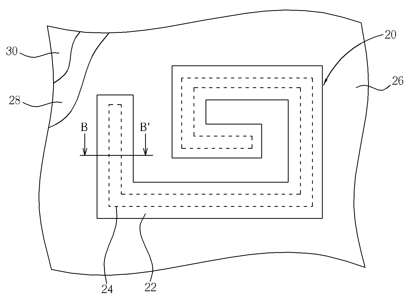
[0029]Please refer to FIGS. 3-5. FIG. 3 shows a schematically plan view of the first embodiment according to the present invention. FIG. 4 shows a schematically cross-sectional view along line B-B′ in FIG. 3. FIG. 5 shows a schematically partial perspective view of the conductor structure shown in FIG. 3. The inductor structure 20 is located in a semiconductor substrate 30. The semiconductor substrate 30 comprises a topmost interconnect (not shown) in a first dielectric layer 26, a second dielectric layer 28 under the first dielectric layer, and at least one via (not shown) in the second dielectric layer and filled with a via plug (not shown) connecting the topmost interconnect. The inductor structure 20 comprises a first conductive layer 22 and a second conductive layer 24. The first conductive layer 22 is in a spiral shape, disposed in the first dielectric layer 26, and comprises a same material as the topmost interconnect. The second conductive layer 24 is filled in a trench open...

second embodiment

[0037]Please refer to FIG. 6 showing a cross-sectional view of the second embodiment according to the present invention. The inductor structure 31 is located in a semiconductor substrate 30. The semiconductor substrate 30 comprises a topmost interconnect (not shown) in a first dielectric layer 26, a second dielectric layer 28 under the first dielectric layer, and at least one via (not shown) in the second dielectric layer and filled with a via plug (not shown) connecting the topmost interconnect. The inductor structure 31 comprises a first conductive layer 32 and two second conductive layers 34a and 34b. The first conductive layer 32 is in a spiral shape, disposed in the first dielectric layer 26, and comprises a same material as the topmost interconnect. The second conductive layers 34a and 34b are respectively filled in two trench openings in the second dielectric layer 28 beneath the first conductive layer 32 and connect the bottom of the first conductive layer 22 with their tops...

third embodiment

[0039]Please refer to FIG. 7, showing a cross-sectional view of the third embodiment according to the present invention. The inductor structure 40 is located in a semiconductor substrate 30. The semiconductor substrate 30 is as described above. The inductor structure 40 comprises a first conductive layer 42 and a second conductive layer 44. The first conductive layer 42 is in a spiral shape, disposed in the first dielectric layer 26, and comprises a same material as the topmost interconnect. The second conductive layer 44 is filled in a trench opening in the second dielectric layer 28 beneath the first conductive layer 42 and connects the bottom of the first conductive layer 42 with its top. The second conductive layer 44 has a same shape as the spiral shape which the first conductive layer 42 has and comprises a same material as the via plug.


PUM

PropertyMeasurementUnit
thicknessaaaaaaaaaa
widthaaaaaaaaaa
widthaaaaaaaaaa

Abstract

An inductor structure is disclosed in the present invention. The inductor structure is formed in a semiconductor substrate, in which a spiral first conductive layer and the topmost interconnect of a multilevel interconnection structure are simultaneously formed in a first dielectric layer, the first conductive layer has the same material as the topmost interconnect has, a second conductive layer and the via plug of the multilevel interconnection structure are simultaneously formed, the second conductive layer is filled in a trench opening in a second dielectric layer, beneath the first conductive layer, and attached to the bottom of the first conductive layer to become an integrated whole. Thus, the cross-sectional area of the conductive layer of the coil is increased and the resistance can be reduced to obtain higher Q factor.

Description

CROSS REFERENCE TO RELATED APPLICATIONS[0001]This application is a division of applicant's earlier application Ser. No. 11 / 552,959, filed on Oct. 25, 2006, which is included herein by reference.BACKGROUND OF THE INVENTION[0002]1. Field of the Invention[0003]The present invention relates to an inductor structure, and particularly to an inductor structure formed in a semiconductor integrated circuit.[0004]2. Description of the Prior Art[0005]In the semiconductor industry, inductors built on silicon substrates are widely used in CMOS based RF circuits such as low-noise amplifiers, voltage-controlled oscillators, and power amplifiers. Conventional inductors that are created on the surface of a substrate are in a spiral shape, formed by semiconductor processes, such as sputtering and etching processes.[0006]FIG. 1 shows a schematic plan view of a conventional inductor in a semiconductor integrated circuit. The inductor is fabricated using an interconnection structure manufacturing proces...

Claims


Application Information

Patent Timeline
Patent Type & Authority Applications(United States)
IPC IPC(8): H01F5/00
CPCH01F17/0006H01F17/0013H01L23/5227H01F2017/0073H01F27/34H01L2924/0002H01L2924/00
Inventor CHEN, CHIH-HUA
Owner UNITED MICROELECTRONICS CORP
Why Eureka
Try Eureka