Release strategies for making transferable semiconductor structures, devices and device components

Active Publication Date: 2008-05-08
THE BOARD OF TRUSTEES OF THE UNIV OF ILLINOIS
View PDF47 Cites 460 Cited by
  • Summary
  • Abstract
  • Description
  • Claims
  • Application Information

AI Technical Summary

Benefits of technology

[0004] Methods and related systems are provided to facilitate low-cost generation of structures capable of printing on device substrates or device components on device substrates. This is accomplished by providing stacks of multilayer structures configured to provide access to individual layers. Of particular use are individual layers that are functional layers, where the functional layers are subsequently incorporated into device and device components. Individual layers are accessed by release strategies that provide sequential layer

Problems solved by technology

This results in a significant decrease in manufacturing cost per solar ce

Method used


Image

  • Release strategies for making transferable semiconductor structures, devices and device components
  • Release strategies for making transferable semiconductor structures, devices and device components
  • Release strategies for making transferable semiconductor structures, devices and device components

Examples


example 1

Release of Transferable Structures for Photovoltaics, Electronics and LEDs

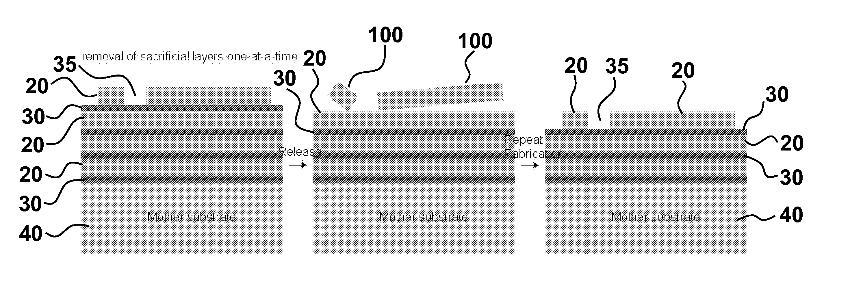
[0094]FIG. 3A-B schematically illustrate methods and structures for simultaneous removal of multiple release layers (FIG. 3A) and sequential layer-by-layer removal of release layers (FIG. 3B). In FIG. 3A, a portion of the multilayer structure 10 is exposed to etchant means, thereby forming an etched access passage 35. Passage 35 provides simultaneous access to a plurality of release layers 30 (three, in this example). In this manner, a plurality of transferable structures 100 are available for printing to a surface of interest, such as a device substrate or device component supported by a substrate by any means known in the art (e.g., liquid printing, contact printing, etc.).

[0095]FIG. 3B summarizes layer-by-layer removal, where etchant access channel 35 spans only the top-most functional layer 20 so that only a single functional layer 20 is released to provide transferable structures 100 from one singly fun...

example 2

Release of Transferable Structures by Laser Ablation

[0103] Other release methods include release by removal of the mother substrate by grinding / polishing / etching or release by thermal shock (e.g. by thermal expansion coefficient mismatch). Release may also be by ablation / decomposition / chemical reaction of embedded layers, such as ablation / decomposition / chemical reaction caused by laser-induced heating. FIG. 6A provides a schematic illustration of a laser ablation release method. Electromagnetic radiation is introduced through an at least partially transparent substrate 40 upon which functional layer 20 is supported, such as by a laser positioned on the side of substrate 40 that is opposite the surface upon which the multilayer structure rests. Laser-induced heating causes release of transferable FMED 100 either by failure of interfacial surface between 20 and 40 or by at least partial removal of a laser-ablating sensitive release surface 30. Release surface 30 may remain partially ...

example 3

Release of Transferable Structures by Propagation of an Induced Interfacial Crack

[0104] Another release mechanism is by introducing a crack at an interface between FMEDs and the mother substrate and then pulling the FMEDs away from the mother substrate (e.g. using a rubber stamp) to propagate the crack (see FIG. 7A). The crack can be introduced in any number of manners, such as mechanically (e.g. by cutting; see FIGS. 8B-C and 12), chemically (e.g. by etching) (see FIGS. 7B and 11), or thermally (e.g. by shock induced by thermal expansion coefficient mismatch).

[0105] Optionally, any of the above means for releasing a transferable structure is combined with a carrier structure, for example a carrier film (FIG. 8A), such as a gold film as a carrier structure for printing carbon nanotubes (see Nature Nanotech. Vol 2, p. 230). This process can be effective for FEMDs that are small (e.g., less than about 50 nm, e.g. molecules, SWNT, etc.) chemically fragile, mechanically fragile, mecha...


PUM


Abstract

Provided are methods for making a device or device component by providing a multilayer structure having a plurality of functional layers and a plurality of release layers and releasing the functional layers from the multilayer structure by separating one or more of the release layers to generate a plurality of transferable structures. The transferable structures are printed onto a device substrate or device component supported by a device substrate. The methods and systems provide means for making high-quality and low-cost photovoltaic devices, transferable semiconductor structures, (opto-)electronic devices and device components.

Description

CROSS-REFERENCE TO RELATED APPLICATIONS [0001] This application claims the benefit of U.S. Provisional Application Nos. 60 / 826,354, filed Sep. 20, 2006 and 60 / 944,653 filed Jun. 18, 2007, each of which are incorporated by reference to the extent they are not inconsistent with the present disclosure.STATEMENT REGARDING FEDERALLY SPONSORED RESEARCH OR DEVELOPMENT [0002] This invention was made with government support under Grant DEFG02-91-ER45439 awarded by Department of Energy. The government has certain rights in the invention.BACKGROUND OF THE INVENTION [0003] A variety of platforms are available for printing structures on device substrates and device components supported by device substrates, including nanostructures, microstructures, flexible electronics, and a variety of other patterned structures. For example, a number of patents and patent applications describe different methods and systems for making and printing a wide range of structures, including U.S. patent application S...

Claims


Application Information

Patent Timeline
IPC IPC(8): H01L31/18H01L21/30
CPCB81C1/0046Y10T156/1195H01L21/7813H01L29/155H01L29/20H01L31/068H01L31/0687H01L31/072H01L31/0725H01L33/0079Y02E10/544Y02E10/547B82Y10/00B82Y20/00H01L31/1844H01L31/03046H01L31/0735H01L31/184B82Y40/00H01L2924/0002B81C2201/0191H01L2924/00H01L33/0093Y02E10/52H01L21/6835H01L2221/68368H01L2224/95001H01L2924/13091Y02P70/50H01L21/82
Inventor ROGERS, JOHN A.NUZZO, RALPH G.MEITL, MATTHEWKO, HEUNG CHOYOON, JONGSEUNGMENARD, ETIENNEBACA, ALFRED J.
Owner THE BOARD OF TRUSTEES OF THE UNIV OF ILLINOIS
Why Eureka
Try Eureka