Semiconductor device and method for manufacturing the same
- Summary
- Abstract
- Description
- Claims
- Application Information
AI Technical Summary
Benefits of technology
Problems solved by technology
Method used
Image

Examples
first embodiment
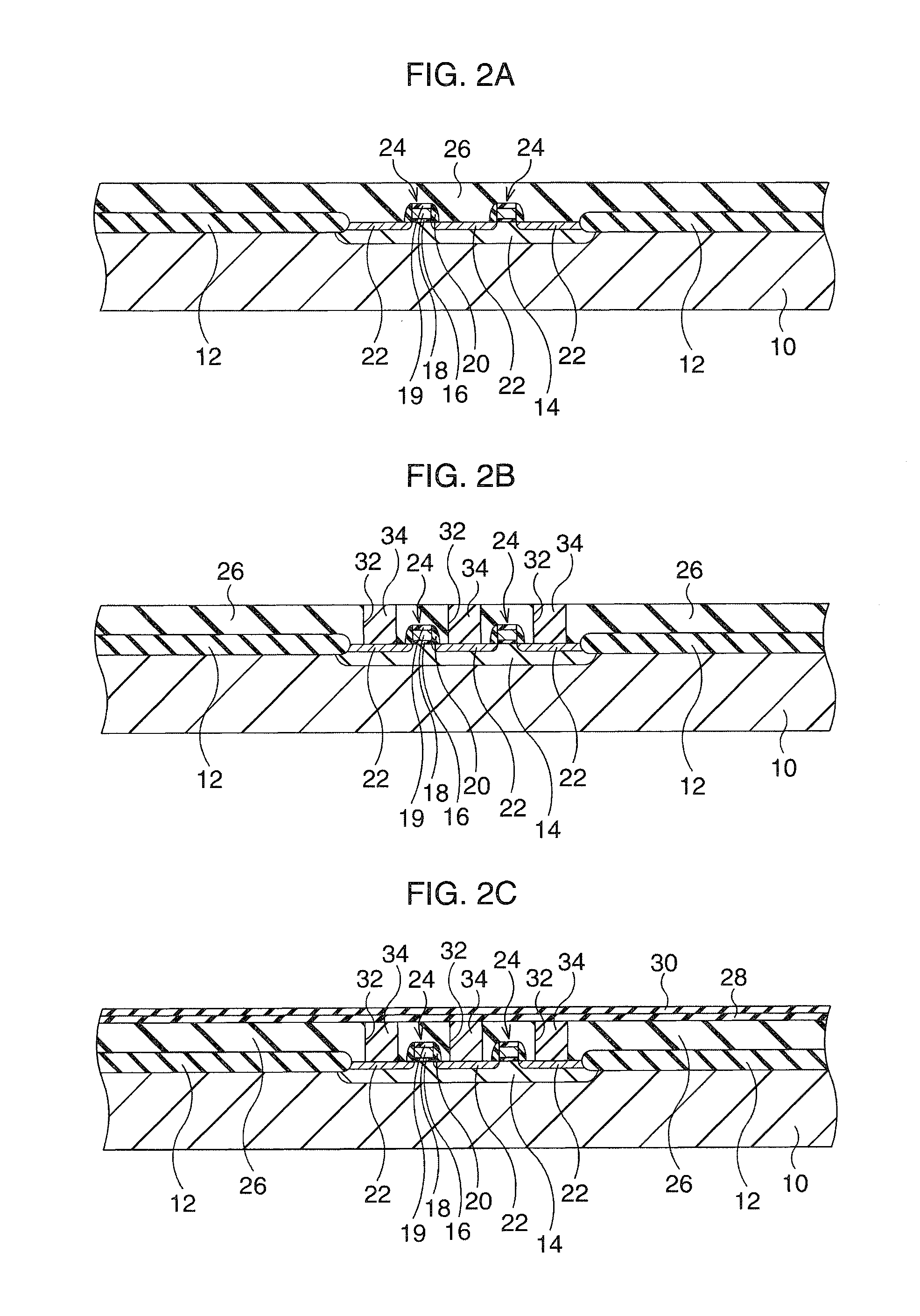
[0046] Next, a first embodiment will be described. Here, the cross-sectional structure of a semiconductor device will be described with a manufacturing method of it for convenience. FIGS. 2A to 2L are sectional views showing a method for manufacturing a ferroelectric memory (semiconductor device) according to the first embodiment in sequence of process steps.
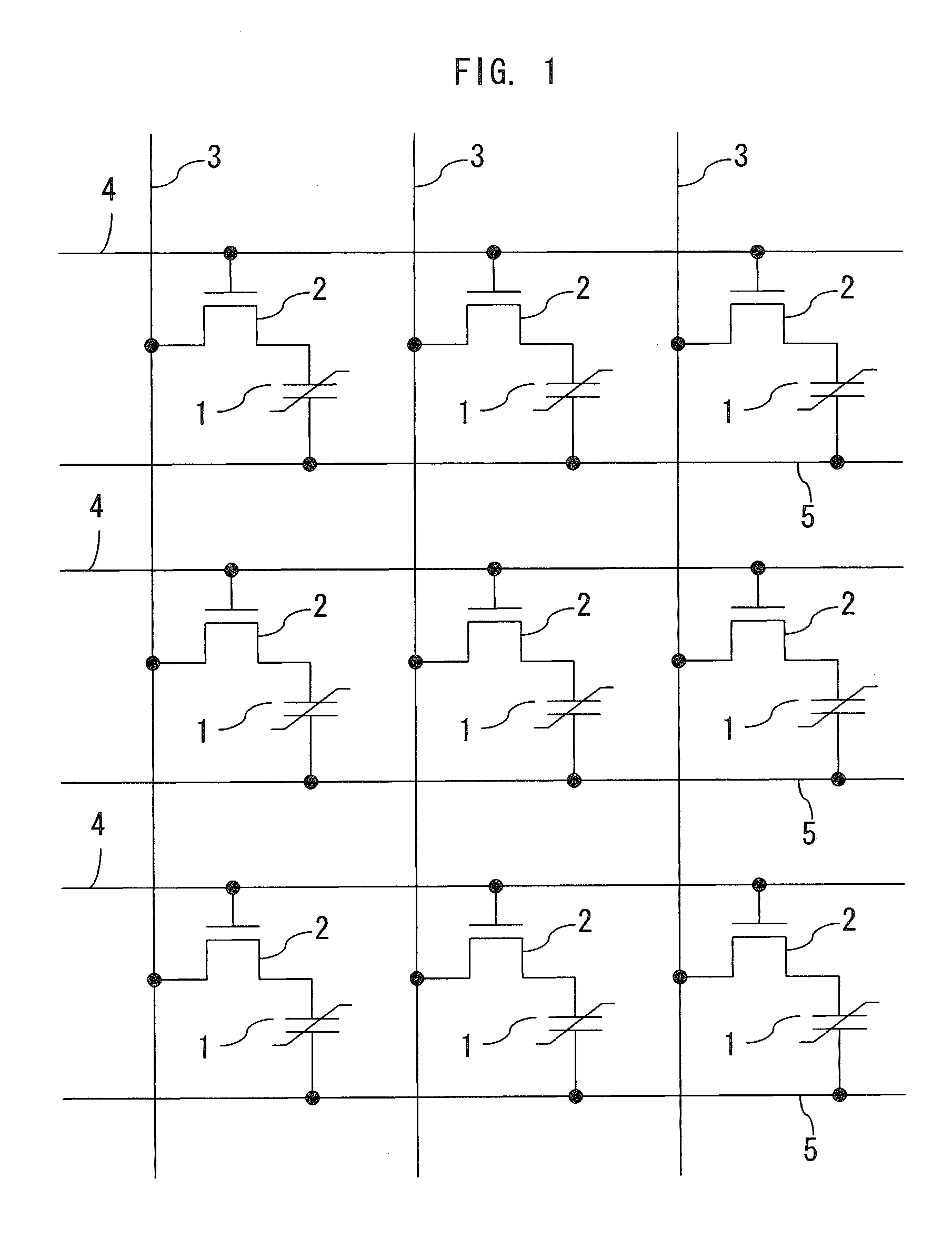
[0047] First, as shown in FIG. 2A, an element isolation region 12 which defines an element region is formed on a semiconductor substrate 10 such as a silicon substrate by, for example, an LOCOS (Local Oxidation of Silicon) method. Next, by introducing a dopant impurity by an ion implanting method, a well 14 is formed. Next, transistors 24 each including a gate insulating film 16, a gate electrode (gate wiring) 18, an insulating film 19, a side wall insulating film 20 and source / drain diffusion layers 22 are formed in the element region. The transistor 24 corresponds to the MOS transistor 2 in FIG. 1.
[0048] Next, an SiON film (...
second embodiment
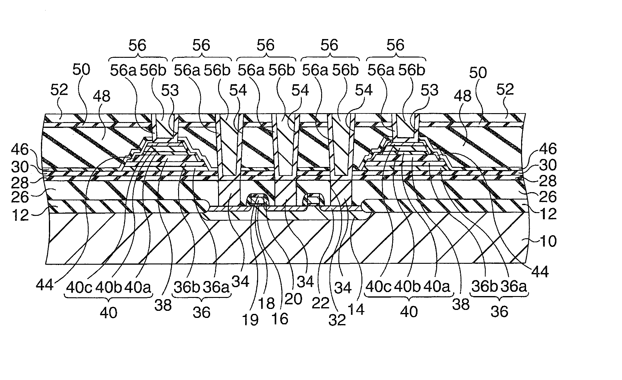
[0110] Next, a second embodiment will be described. FIG. 4 is a sectional view showing a ferroelectric memory (semiconductor device) according to the second embodiment.
[0111] In the second embodiment, a barrier film 84 is formed between the wiring (first metal wiring layer) 58 and the wiring (second metal wiring layer) 66, and a barrier film 86 is formed between the wiring (second metal wiring layer) 66 and a wiring (third metal wiring layer) 76. In other words, on the flattened silicon oxide film 62, the barrier film 84 and the silicon oxide film 65 are sequentially formed, and the wiring 66 is formed thereon. Further, on the flattened silicon oxide film 70, the barrier film 86 and the silicon oxide film 71 are sequentially formed, and the wiring 76 is formed thereon. The barrier films 84 and 86 are aluminum oxide films each of a thickness of 50 nm, for example. The thickness of each of the silicon oxide films 65 and 71 is, for example, 100 nm.
[0112] When the semiconductor device...
third embodiment
[0116] Next, a third embodiment will be described. In each of the first and the second embodiments, the structure of the ferroelectric capacitor 42 is of a planar type, but in the third embodiment, a ferroelectric capacitor of a stacked structure is provided. Hereinafter, the third embodiment will be described in detail, and its sectional structure will be described with its manufacturing method for convenience. FIGS. 5A to 5F are sectional views showing a method for manufacturing a ferroelectric memory (semiconductor device) according to the third embodiment in sequence of process steps.
[0117] In this embodiment, as shown in FIG. 5A, a well 312 is first formed on a surface of a semiconductor substrate 311 such as a silicon substrate. An element isolation region 313 is formed on the surface of the semiconductor substrate 311 by, for example, STI (shallow trench isolation). Subsequently, a gate insulating film 314, a gate electrode 315, a cap film 316, a side wall 317, source / drain ...
PUM
 Abstract
Description
Claims
Application Information
 - R&D Engineer
- R&D Manager
- IP Professional
- Industry Leading Data Capabilities
- Powerful AI technology
- Patent DNA Extraction
Browse by: Latest US Patents, China's latest patents, Technical Efficacy Thesaurus, Application Domain, Technology Topic.
© 2024 PatSnap. All rights reserved.Legal|Privacy policy|Modern Slavery Act Transparency Statement|Sitemap