
Coating material based on a copper-indium-gallium alloy, in particular for the production of sputter targets, tubular cathodes and the like

a technology of copper-indium-gallium alloy and coating material, which is applied in the direction of liquid/solution decomposition chemical coating, vacuum evaporation coating, coating, etc., can solve the problems of lack of cu, inability to obtain constant results in the composition of layers over a longer period of time, and inability to achieve uniform distribution of elements

Inactive Publication Date: 2008-05-29
GFE METALLE & MATERIALIEN GMBH
View PDF4 Cites 19 Cited by
  • Summary
  • Abstract
  • Description
  • Claims
  • Application Information

AI Technical Summary

Benefits of technology

[0020]It is the object of the present invention to provide a coating material which allows for vapour deposition of CIG layers in one single step. By using an evaporation source possessing the correct composition, a high electrical conductivity and a melting point higher than 200° C., this process is reduced to a PVD coating step. The desired composition of the layer is then no longer a problem, selenization may subsequently occur by evaporation, as usual.

Problems solved by technology

With these processes, however, constant results with regard to the composition of the layers can hardly be obtained over a longer period of time.
One problem is for example a lack of Cu during the use of these methods or a non-uniform distribution of the elements used.
Moreover, several steps are often required for depositing the CIG layer since it is impossible to deposit all three elements by sputtering.
The melting point of Ga, for example, is 30° C., which inevitably causes the Ga-metal to melt and drip off during the coating process.
Due to the semiconducting properties of this metal, the electrical conductivity is very low.
Consequently, the coating process is disrupted.
The current state of the art allows for sputter targets, both planar and in the shape of a tubular cathode, to be developed by using the three components Cu, In and Ga in order to create the semiconducting CIGS layers; these sputter targets, however, possess a plurality of infavourable material properties and very poor sputtering and layer properties due to an inappropriate conduction of heat during the production of the ternary coating material.
The efficiency of the solar cells thus obtained is too low.Further methods involving electroplating or screen printing processes for the deposition of the individual layers are still being tested.
A sputter target incorporating the three elements Cu, in and Ga at the desired proportion has not been successfully used in any of the above “conventional” methods of production.

Method used


Image

  • Coating material based on a copper-indium-gallium alloy, in particular for the production of sputter targets, tubular cathodes and the like
  • Coating material based on a copper-indium-gallium alloy, in particular for the production of sputter targets, tubular cathodes and the like
  • Coating material based on a copper-indium-gallium alloy, in particular for the production of sputter targets, tubular cathodes and the like

Examples


Embodiment Construction

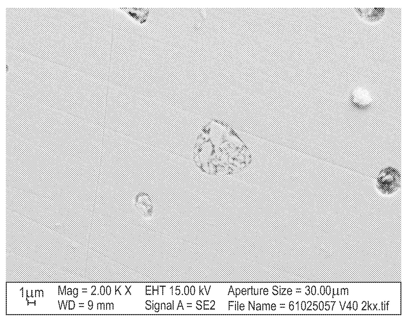
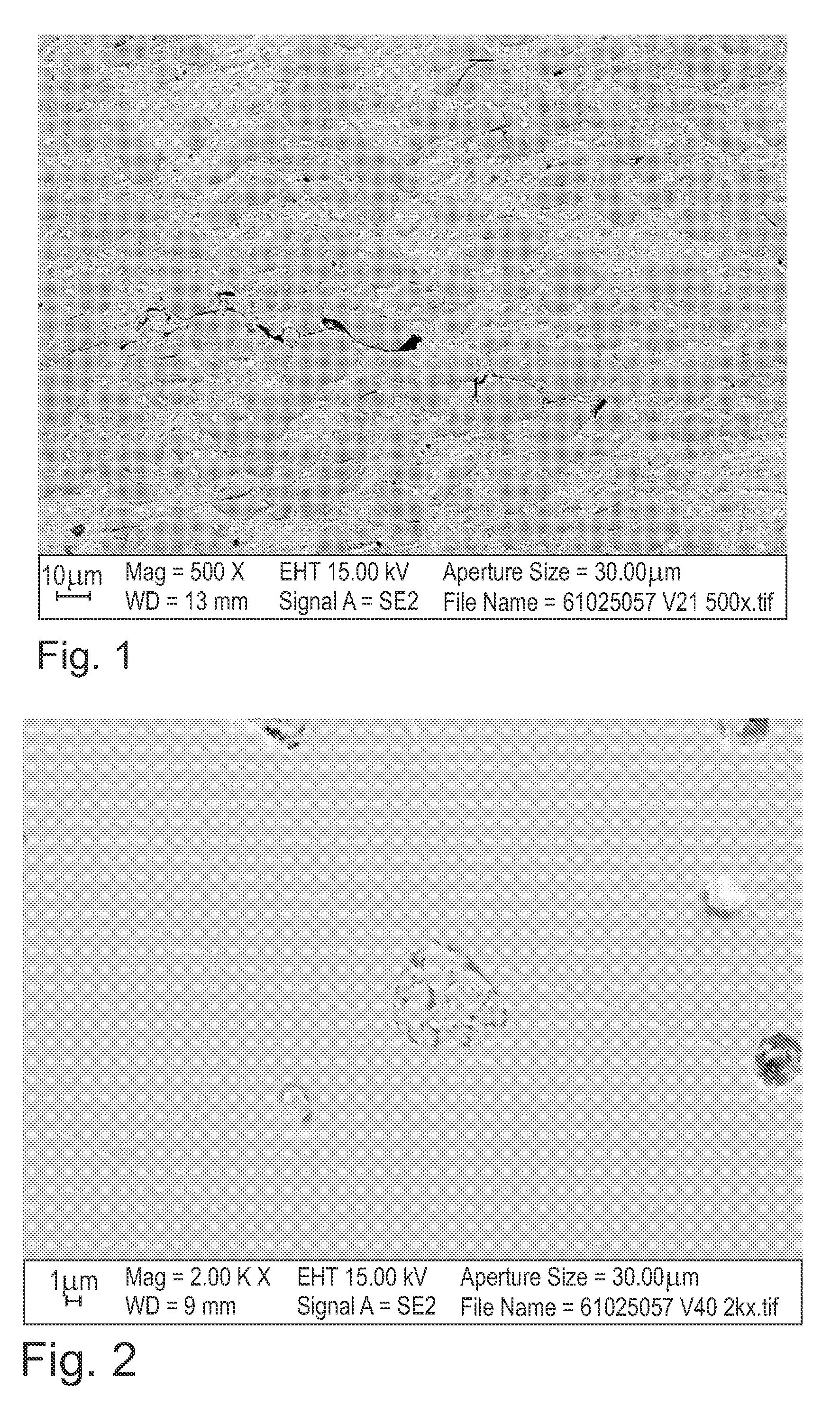
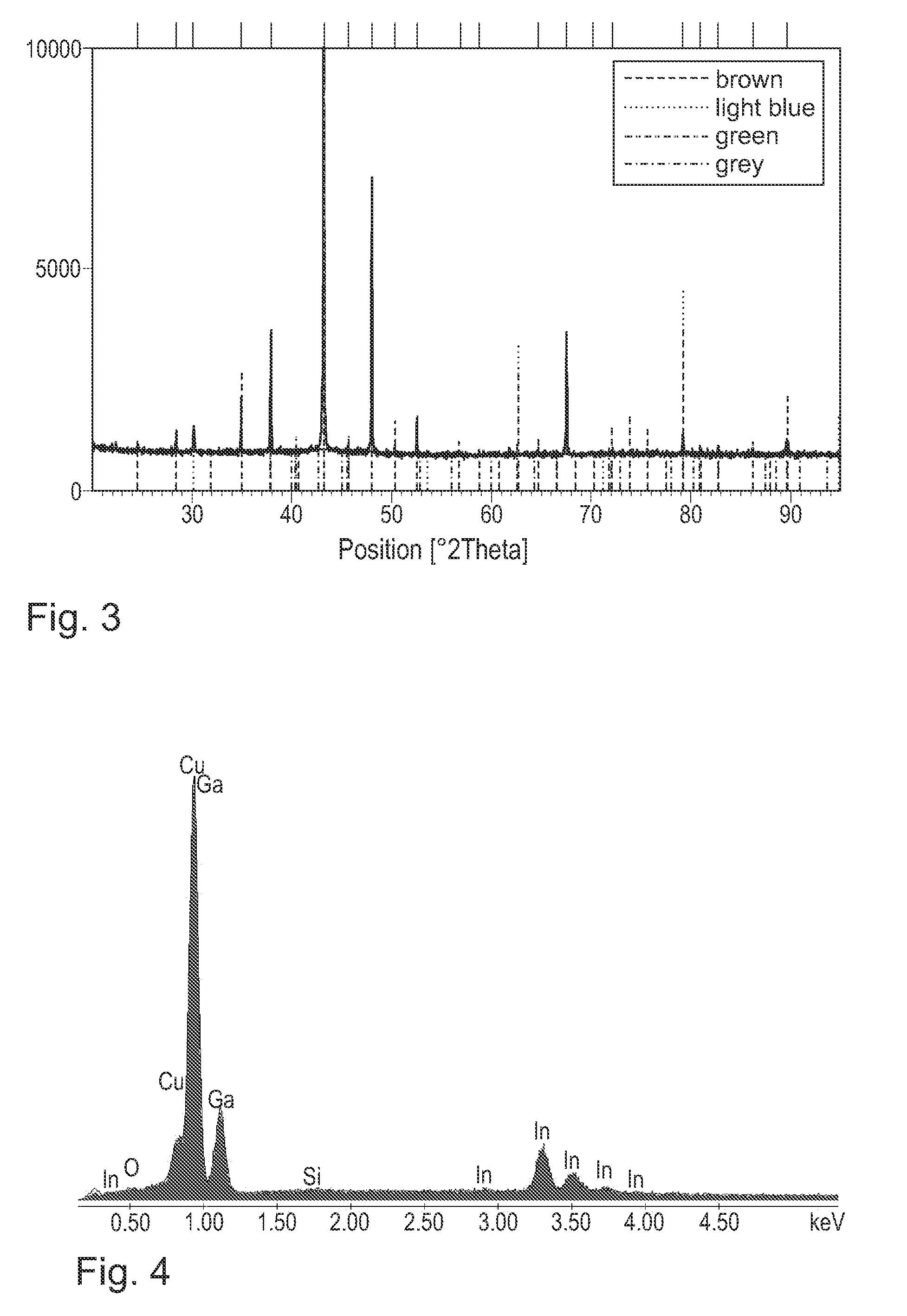
[0045]When a defined alloy composition and conduction of heat as well as solidification rate are provided, a cubic phase of the Cu5Zn8 prototype phase lattice type is formed in molten CuInGa alloys, with gallium, in this case, occupying the site of the zinc.

[0046]Indium is dissolved in this phase at a proportion of up to 22 weight percent (wt %). If the indium concentration exceeds 25 wt %, precipitation occurs, resulting in the formation of the matrix surrounding the above mentioned phase. If the copper concentration exceeds 63 wt %, indium and gallium are either dissolved in Cu or combine with copper to form the following binary compounds:

PhaseStability range in KCu2Gaγ1298-918Cu2Gaγ 763-1109Cu3Gaβ 298-1188Cu5Ga3γ2298-758Cu7Ga2ζ′298-595Cu7Ga2ζ603-893Cu7In4δ298-904Cu7Inβ847-983

[0047]The binary alloy system InGa does not form phases but a low-melting eutectic mixture at 15° C.

[0048]This can be taken from the literature listed below:[0049]“Constitution Of Binary Alloys”, Hansen, 2. e...


PUM


Abstract

The copper-indium-gallium (CuInGa) alloy is in particular to be used for the production of sputter targets, tubular cathodes and similar coating material sources. It has a phase corresponding to a Cu5Zn8 prototype phase in which the lattice sites of the zinc atoms (Zn) are occupied by gallium atoms (gallium-substituted Cu5Zn8 phase) and in which indium is simultaneously introduced into the elementary cell or phase, making up a proportion of up to 26 wt %.

Description

BACKGROUND OF THE INVENTION[0001]1. Field of the Invention[0002]The invention relates to a coating material based on a copper-indium-gallium (CuInGa) alloy, in particular for the production of sputter targets, tubular cathodes and similar coating material sources.[0003]2. Background Art[0004]The production of a CuInGa alloy by ingot metallurgy is in principle known from DE 698 35 851 T2. The composition of the alloy mentioned there substantially equals those of the invention disclosed in the following. EP 0 308 201 A1 relates to a sputter target to be used in the production process of magneto-optical recording media. Correspondingly, U.S. Pat. No. 6,682,636 B2 discloses PVD targets and methods of producing them. However, neither of the two disclosures teaches the use of a CuInGa alloy as a coating material.[0005]Field of application is the production of thin-film solar cells with a semiconductor layer consisting of CuInGaSe2 or CuInGaS2 (common abbreviation CIGS). In this process, a...

Claims


Application Information

Patent Timeline
IPC IPC(8): C09D5/00
CPCC23C14/3414
Inventor VAN OSTEN, KARL-UWEBRITTING, STEFAN
Owner GFE METALLE & MATERIALIEN GMBH
Learn More