Organic thin film transistor with dual layer electrodes

Active Publication Date: 2008-05-29
SAMSUNG ELECTRONICS CO LTD
View PDF19 Cites 6 Cited by
  • Summary
  • Abstract
  • Description
  • Claims
  • Application Information

AI Technical Summary

Benefits of technology

[0009]The source and drain electrodes each comprise first and second layers. Each first layer comprises a material having a work function differing from the energy level of the semiconductor layer by at least 0.5 eV. Each second layer comprises a material

Problems solved by technology

TFT circuits using current mainstream silicon technology may be too costly for some applications, particularly for large-area electronic devices such as backplane switching circuits for displays (e.g., active matrix liquid crystal monitors or televisions) and low-end electronic devices such as radio frequency identification (RFID) tags where high swit

Method used


Image

  • Organic thin film transistor with dual layer electrodes
  • Organic thin film transistor with dual layer electrodes
  • Organic thin film transistor with dual layer electrodes

Examples


example 1

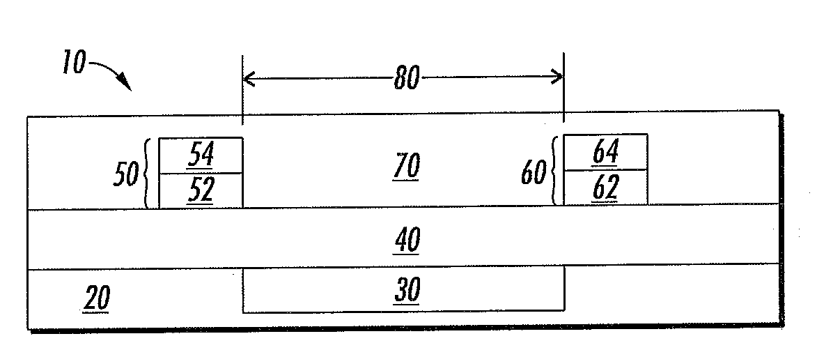
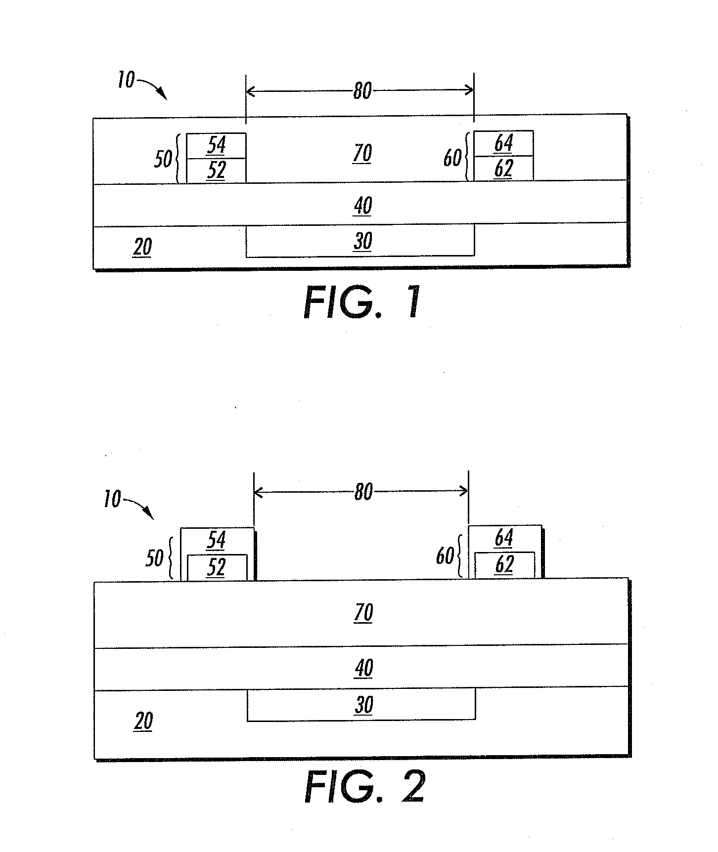
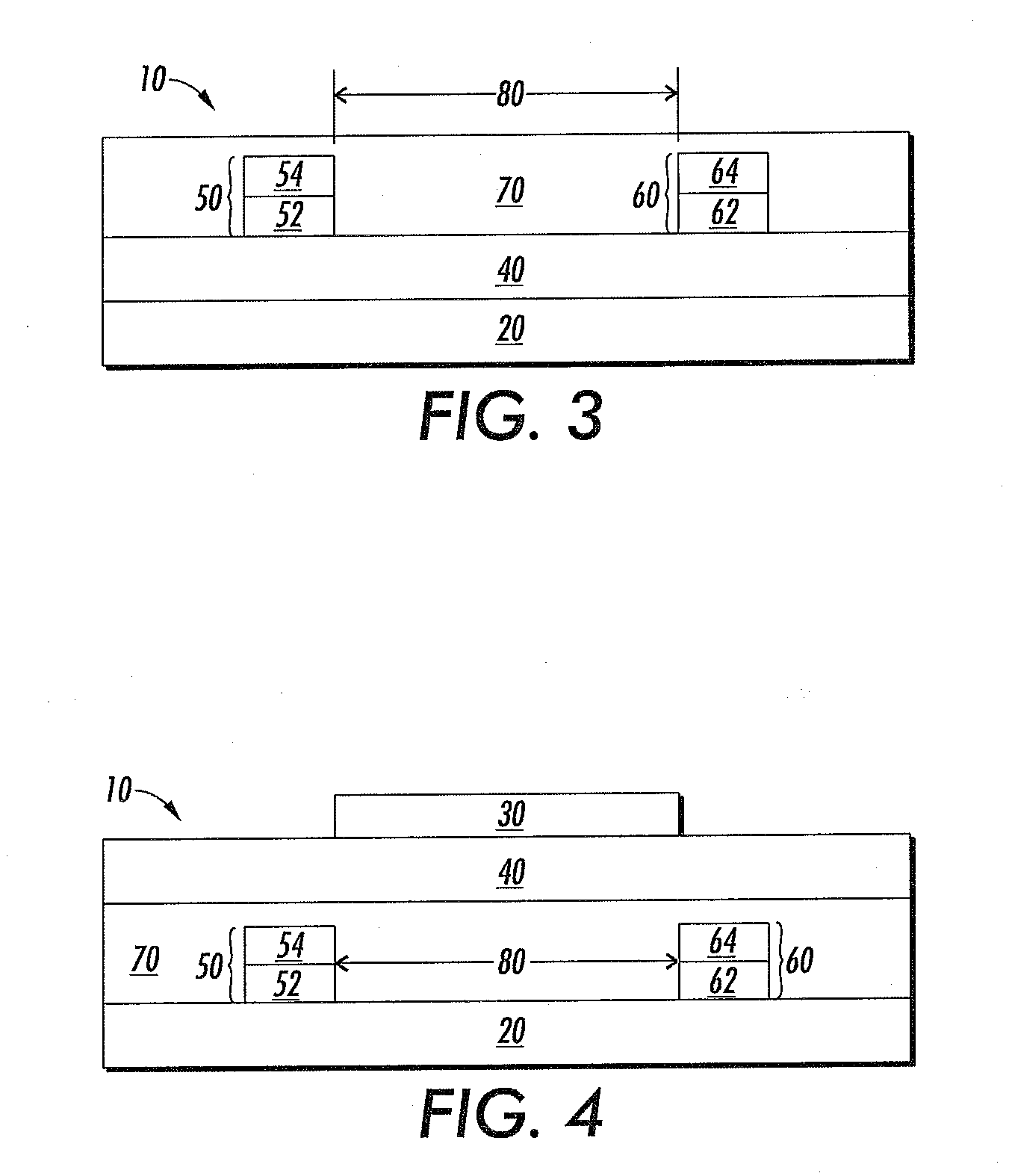
[0052]A bottom-contact thin-film transistor with a configuration illustrated in FIG. 3 was built. It comprised an n-doped silicon wafer with a thermally grown silicon oxide layer having a thickness of about 300 nanometers. The wafer functioned as the gate electrode. The silicon oxide layer functioned as the gate dielectric layer. A 10-nanometer layer of titanium was applied in two locations corresponding to the source and drain electrodes. This titanium layer was the first layer of the dual-layer electrodes. Next, a 100-nanometer layer of gold was applied to the titanium layers to form the second layer of the dual-layer electrodes. The semiconductor channel length (i.e. distance between the source and drain electrodes) was 5 microns.

[0053]The silicon oxide surface was modified with octyltrichlorosilane (OTS-8) by immersing the devices in 0.1 M OTS-8 solution in toluene at 60° C. for 20 min. The gold surface was then modified with octanethiol by immersing the devices in 0.01 M octane...


PUM

PropertyMeasurementUnit
Thicknessaaaaaaaaaa
Thicknessaaaaaaaaaa
Thicknessaaaaaaaaaa

Abstract

A thin-film transistor (TFT) with dual-layer source and drain electrodes is provided. Each source and drain electrode comprises a first layer and a second layer. The first layer has a work function which differs from the energy level of the semiconductor by at least 0.5 eV and the second layer has a work function matching the energy level of the semiconductor. The semiconductor has a short channel length.

Description

BACKGROUND[0001]The present disclosure relates, in various embodiments, to multilayer electrodes and thin-film transistors (TFTs) comprising the same.[0002]TFTs are fundamental components in modern-age electronics, including, for example, sensor, imaging, and display devices. TFT circuits using current mainstream silicon technology may be too costly for some applications, particularly for large-area electronic devices such as backplane switching circuits for displays (e.g., active matrix liquid crystal monitors or televisions) and low-end electronic devices such as radio frequency identification (RFID) tags where high switching speeds and / or high density are not essential. The high costs of silicon-based TFT circuits are primarily due to the capital-intensive silicon fabrications as well as the complex high-temperature, high-vacuum photolithographic fabrication processes under strictly controlled environments needed to make them. Because of the cost and complexity of fabricating sil...

Claims


Application Information

Patent Timeline
IPC IPC(8): H01L51/05H01L29/786
CPCH01L51/0037H01L51/0525H01L51/105H01L51/0545H01L51/0541H10K85/1135H10K10/472H10K10/464H10K10/84H10K10/466H01L29/458
Inventor WU, YILIANGONG, BENG S.
Owner SAMSUNG ELECTRONICS CO LTD
Why Eureka
Try Eureka