

Vertical electrical device
a vertical electrical device and vertical technology, applied in the direction of fixed capacitor dielectrics, structural fixed capacitor combinations, fixed capacitor details, etc., can solve the problems of insufficient isolation and/or signal transmission characteristics for high frequency operation, inability to achieve high frequency performance, etc., to achieve the effect of optimizing the radio frequency properties of the devi
- Summary
- Abstract
- Description
- Claims
- Application Information
AI Technical Summary
Benefits of technology
Problems solved by technology
Method used
Image

Examples
Embodiment Construction
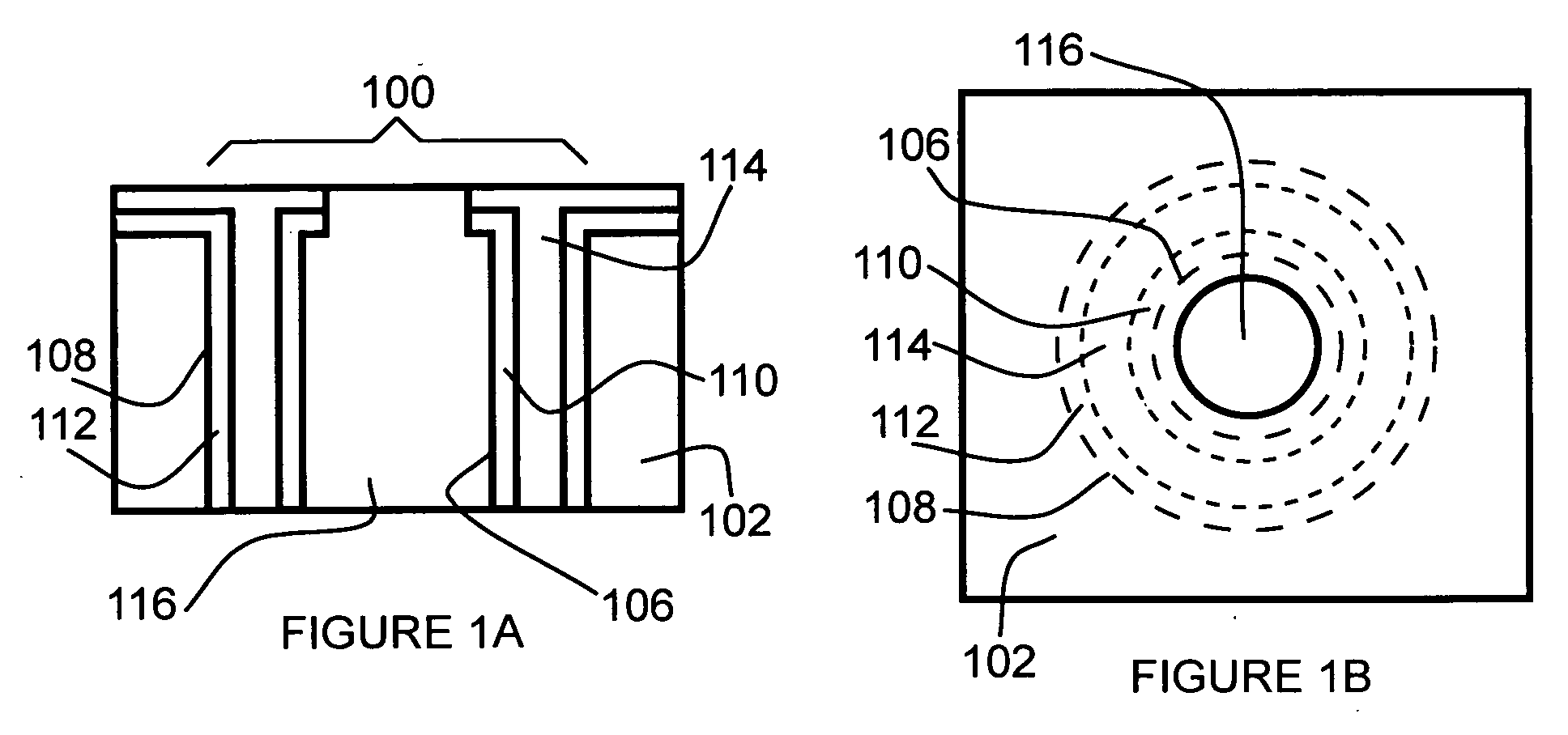
[0035]FIGS. 1A and 1B depict a vertical electrical device constructed according to the invention, with FIG. 1A showing a cross sectional view of the device in a side elevation and FIG. 1B a plan view. A region 100 extends into a substrate 102. The region is defined by an inner wall 106 and an outer wall 108 circumscribing the inner wall.
[0036]An inner electrically conductive layer 110 is disposed on the inner wall 106 and an outer electrically conductive layer 112 is disposed on the outer wall 108. An electrically insulative material 114 is placed between the inner and outer layers. An electrical conductor 116 in the substrate is bounded by the inner conductive layer 110.
[0037]This device is useful as a via conductor that can be implemented in electronics applications involving 3D architectures and structures that combine multiple layers of semiconductor circuitry or that integrate semiconductor circuitry with other devices. The device is particularly advantageous because it can be ...
PUM
 Abstract
Description
Claims
Application Information