Electron-Emitting Device, Electron Source Using the Same, Image Display Apparatus, and Information Displaying and Reproducing Apparatus

Inactive Publication Date: 2008-05-29
CANON KK
View PDF46 Cites 20 Cited by
  • Summary
  • Abstract
  • Description
  • Claims
  • Application Information

AI Technical Summary

Benefits of technology

[0015]According to the present invention, an electron-emitting device with dramatically improved electron emitting efficiency can be provided. As a result, an image display apparatus and an information displaying and reproducing apparatus with excellent display quality for a long time can be provided.
[0016]Further, according to the present invention, since, when volta

Problems solved by technology

However, an image display apparatus has been recently required to

Method used


Image

  • Electron-Emitting Device, Electron Source Using the Same, Image Display Apparatus, and Information Displaying and Reproducing Apparatus
  • Electron-Emitting Device, Electron Source Using the Same, Image Display Apparatus, and Information Displaying and Reproducing Apparatus
  • Electron-Emitting Device, Electron Source Using the Same, Image Display Apparatus, and Information Displaying and Reproducing Apparatus

Examples


example 1

[0177]The basic structure of an electron-emitting device according to this example is similar to that illustrated in FIGS. 1A to 1C. The basic structure of and a method of manufacturing the device according to this example are described in the following with reference to FIGS. 1A to 1C, 3, and 4A to 4D.

(Process-a)

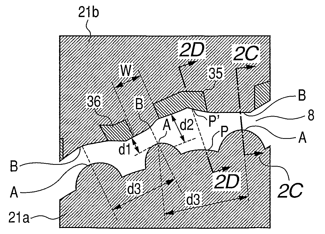
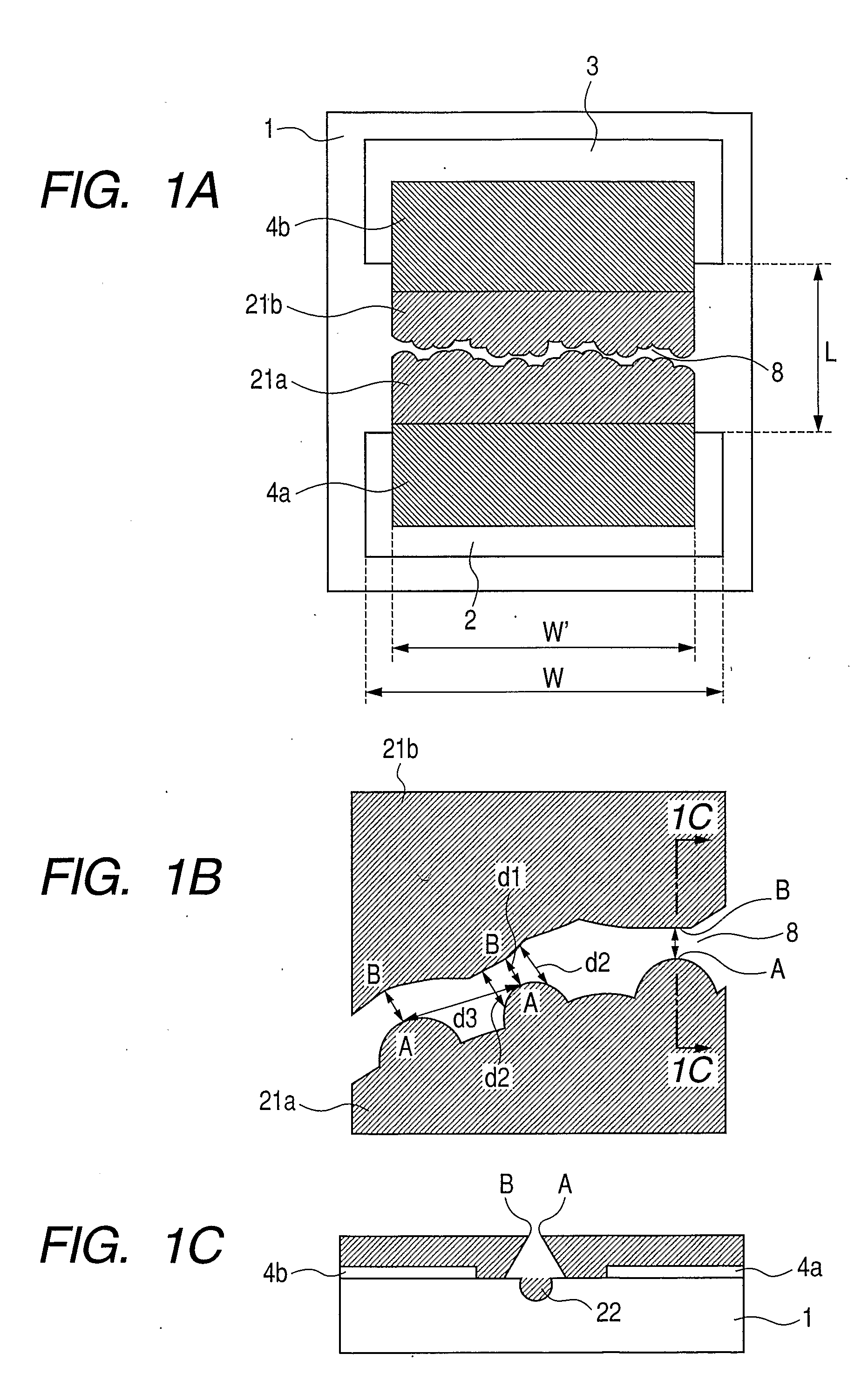
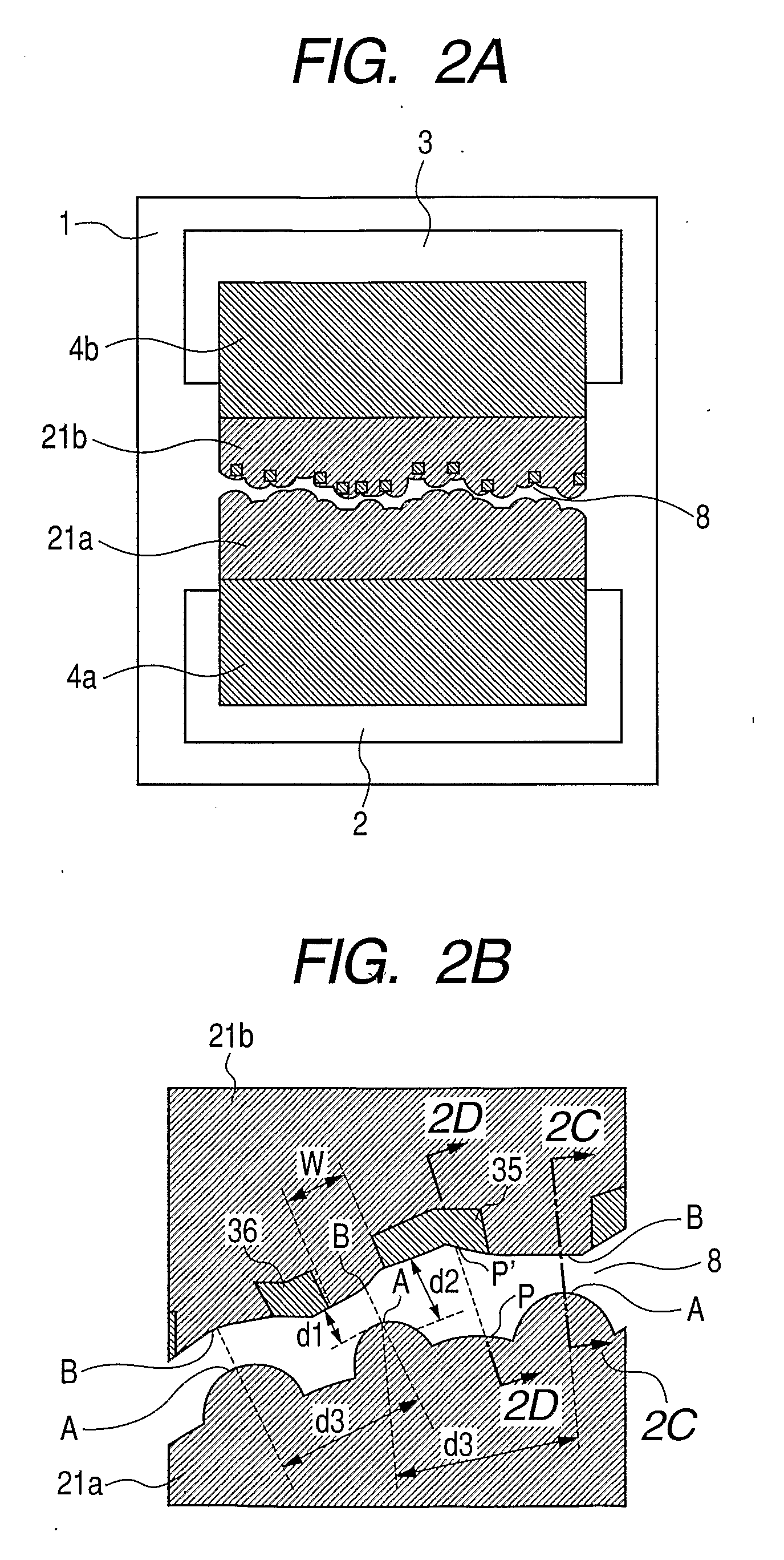
[0178]First, photoresist shaped correspondingly to the pattern of the auxiliary electrodes 2 and 3 was formed on the cleaned quartz substrate 1. Then, Ti at the thickness of 5 nm and Pt at the thickness of 45 nm were deposited in this order by electron beam vapor deposition. The photoresist pattern was dissolved away by organic solvent, the Pt / Ti deposition film was lifted off, and the first and second auxiliary electrodes 2 and 3 in opposition to each other with a length L of 20 μm therebetween were formed. The width W of the auxiliary electrodes 2 and 3 (see FIGS. 1A to 1C) was 500 μm (FIG. 4A).

(Process-b)

[0179]After an organic palladium compound solution was spin coated ...

example 2

[0207]This example is a further preferable example of the present invention.

[0208]In this example, electron-emitting devices were manufactured in the same way as that in Example 1 except that Process-e and Process-f of Example 1 were modified as described in the following. Thus, here, Process-e and Process-f will be described.

(Process-e)

[0209]Following Process-e, in order to carry out the activation process, acrylonitrile was introduced into the vacuum chamber through a slow leak valve. Then, the pulse voltage having the waveform illustrated in FIG. 8B was applied between the auxiliary electrodes 2 and 3 with T1 being 1 msec, T1′ being 0.3 msec, and T2 being 5 msec. The “activation” process was curried out with the first auxiliary electrode 2 fixed at the ground potential and pulse voltage having the waveform illustrated in FIG. 8B was applied to the second auxiliary electrode 3.

[0210]After 120 minutes lapsed from the beginning of the activation process, it was made sure that the gr...

example 3

[0238]In this example, the electron-emitting device illustrated in FIGS. 27A to 27C was manufactured using electron beam irradiation. Since Process-a of this example is the same as Process-a of Example 1, the description thereof is omitted in the following.

(Process-b)

[0239]Next, the substrate 1 having the auxiliary electrodes 2 and 3 formed thereon was disposed in the measurement / evaluation apparatus illustrated in FIG. 3 (with an electron beam irradiating means (not shown)). Then, the measurement / evaluation apparatus was evacuated by a vacuum pump until the vacuum reached 1×10⁻⁶ Pa. After that, acrylonitrile was introduced into the vacuum chamber through a slow leak valve. Then, the electrodes 2 and 3 were set at the ground potential and electron beam irradiation was carried out so that the first and second carbon films 21a and 21b as illustrated in FIGS. 27A to 27C were formed. The acceleration voltage of the electron beam was 5 kV and the current was 10 μA. The width W′ of the ca...


PUM


Abstract

An electron-emitting device is provided with improved electron emitting efficiency. An electron-emitting device includes first and second electroconductive films disposed (21a, 21b) on a surface of a substrate in opposition to each other to form a gap (8) between ends of the first and second electroconductive films. The end of the first electroconductive film includes a portion (A) the minimum distance d1 from which to the second electroconductive film (B) is 10 nm or less. Let d2 denote a minimum distance between the end of the first electroconductive film which is away from the portion the minimum distance d1 from which to the second electroconductive film is 10 nm or less by the minimum distance d1 and the end of the second electroconductive film. The relation of d2/d1≧1.2 is satisfied.

Description

TECHNICAL FIELD[0001]The present invention relates to an electron-emitting device, electron source using the same, and image display apparatus. The present invention also relates to an information displaying and reproducing apparatus such as a television set for receiving a broad casted signal such as television broadcasting, and for displaying and reproducing image information, character information, audio information, which are included in the broad casted signal.BACKGROUND ART[0002]Electron-emitting devices include such as field emission electron-emitting devices and surface conduction electron-emitting devices. As disclosed in Patent Documents 1 to 3, there are some cases where a surface conduction electron-emitting device is performed a process referred to as “activation”. “Activation” process is a process for forming an electroconductive film (typically a carbon film) in a gap between a pair of electroconductive films and on the electroconductive films adjacent to the gap. FIG...

Claims


Application Information

Patent Timeline
IPC IPC(8): H01J1/316
CPCH01J1/316H01J31/127H01J29/481H01J9/025H01J31/12
Inventor NUKANOBU, KOKIMORIGUCHI, TAKUTOYAMAMOTO, KEISUKE
Owner CANON KK
Why Eureka
Try Eureka