

Gate Drive Circuit
a drive circuit and gate technology, applied in the field of gate drive circuits, can solve the problems of large reverse recovery current, increased turn-on loss, reverse recovery loss (err) generated on the element, etc., and achieve the effect of reducing both switching power loss and noise, and reducing the loss of power semiconductor elements
- Summary
- Abstract
- Description
- Claims
- Application Information
AI Technical Summary
Benefits of technology
Problems solved by technology
Method used
Image

Examples
first embodiment
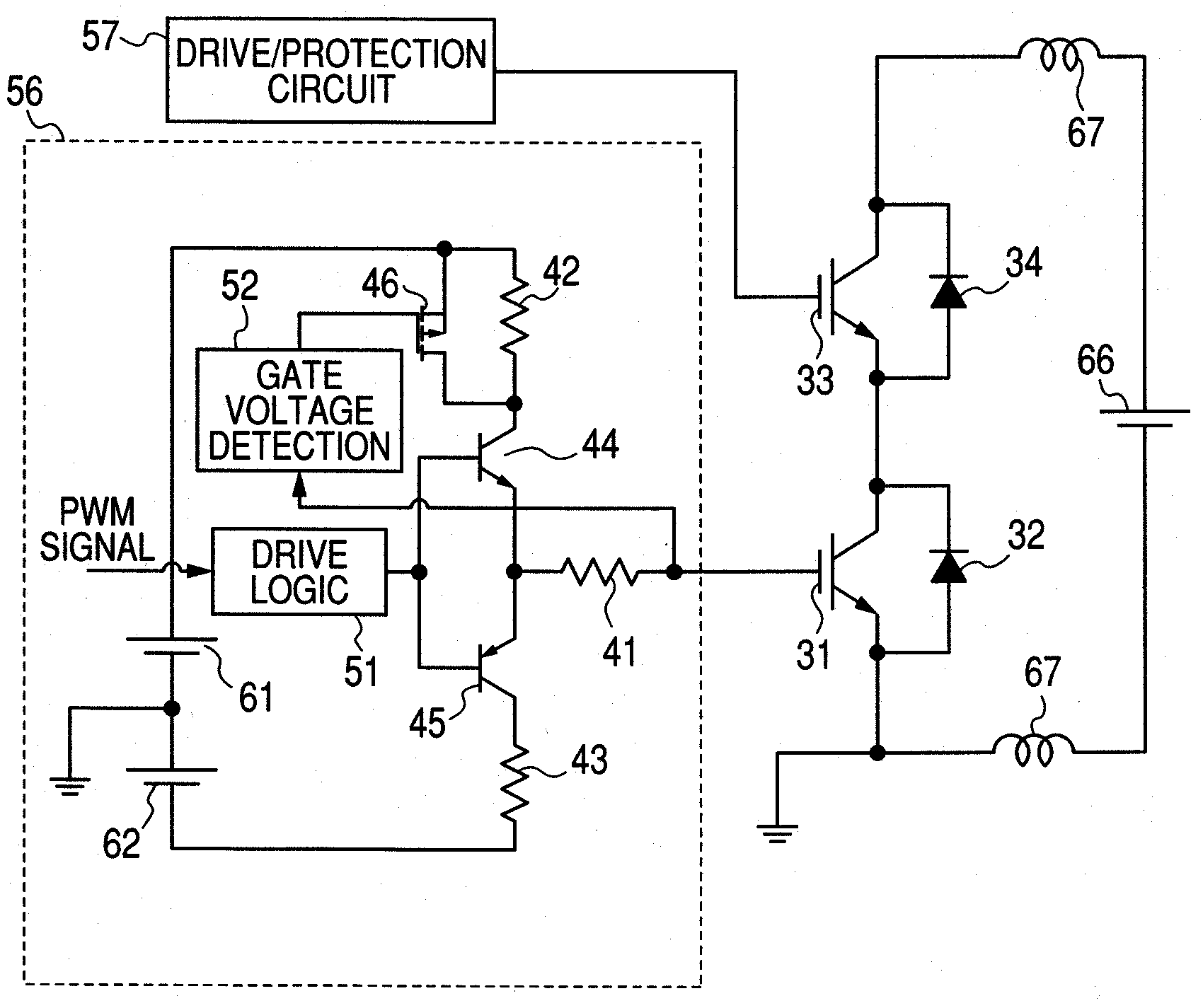
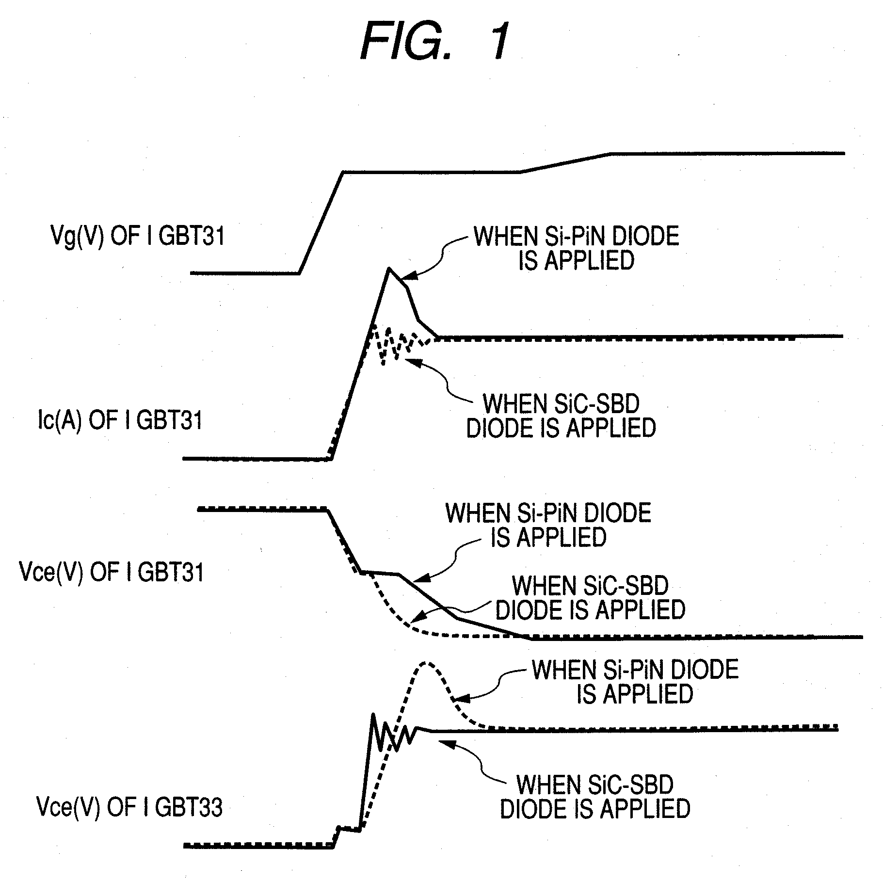
[0061]FIG. 2 shows the configuration of a drive circuit of a power semiconductor element according to a first embodiment of the present invention. The first embodiment relates to a drive circuit which changes gate resistance in two stages.
[0062]The main circuit of an inverter, located on the right in the drawing, comprises lower Si-IGBT 31 and SIC-SBD 32, upper Si-IGBT 33 and SiC-SBD 34, and a main circuit power supply 66. The main circuit's Si-IGBTs 31 and 33 are connected to a lower-side drive / protection circuit 56 and an upper-side drive / protection circuit 57 which drive those Si-IGBTs. In FIG. 2, the detailed configuration of the lower-side drive / protection circuit 56 is shown encircled by the broken line, and the upper-side drive / protection circuit 57 has the same configuration; therefore, the detail is omitted.
[0063]The drive / protection circuit 56 of this embodiment newly comprises a gate voltage detection circuit 52 and a gate resistance switching PMOS 46 in addition to gate ...
second embodiment
[0067]FIG. 4 is a block diagram of a drive circuit of a power semiconductor element according to a second embodiment of the present invention. In the drawing, the same symbol is used for the same component as that of a first embodiment. The difference between this embodiment and the first embodiment shown in FIG. 2 is that this embodiment is equipped with a one-shot pulse generation circuit 53 which inputs the output of a gate voltage detection circuit so as to change gate resistance in three stages.
[0068]Next, operation of a drive / protection circuit 56 according to a second embodiment will be described with reference to FIG. 5. FIG. 5 shows the voltage and current waveform of the lower IGBT 31 and the upper IGBT 33 which changes over time. In the drive / protection circuit 56 according to this embodiment, a one-shot pulse generation circuit 53 is added, and control is executed (resistance: small to large to small) so that gate resistance is increased for a constant period of time. Si...
third embodiment
[0072]FIG. 8 shows the configuration of a drive circuit of a power semiconductor element according to a third embodiment of the present invention. The same symbol is used for the same component as that of a first embodiment. The difference between this embodiment and a second embodiment shown in FIG. 4 is that a speed-up capacitor 47 is added to this embodiment instead of providing a one-shot pulse generation circuit 53. The drive circuit according to a third embodiment changes gate resistance in three stages in the same manner as the second embodiment.
[0073]Next, operation of a drive / protection circuit 56 according to a third embodiment will be explained with reference to FIG. 9. FIG. 9 shows the voltage and current waveform of the lower IGBT 31 and the upper IGBT which changes over time. A speed-up capacitor 47 is added to a circuit of this embodiment to increase gate charging current when the power is initially turned on. That is, when the power is initially turned on, the PMOS 4...
PUM
 Abstract
Description
Claims
Application Information