Test structure

a test structure and structure technology, applied in the direction of semiconductor/solid-state device testing/measurement, semiconductor device details, semiconductor/solid-state device testing/measurement, etc., can solve the problems of short circuit, undesirable electrical connection, small device making up the integrated circuit, etc., to achieve efficient detection and avoid delay in the fabrication process

Active Publication Date: 2008-06-12
TAIWAN SEMICON MFG CO LTD
View PDF2 Cites 16 Cited by
  • Summary
  • Abstract
  • Description
  • Claims
  • Application Information

AI Technical Summary

Benefits of technology

[0014]An advantage of a preferred embodiment of the present invention is that vertical shorts formed in a pad structure, for example by wire bonding or test probe application, may be detected efficiently and without the need for time-consuming and destructive te...

Problems solved by technology

The devices making up the integrated circuits are very small, and there are typically a great number of them on a single chip, which is often less than a square centimeter in area and very thin.
In some instances, however, an undesirable electrical connection, that is, a short circuit, may be caused by a defect in the pad structure.
Despite their relatively-large size compared with other semiconductor devices, the pads are nevertheless fairly small and fragile, and d...

Method used


Image

  • Test structure
  • Test structure
  • Test structure

Examples


Embodiment Construction

[0026]The making and using of the presently preferred embodiments are discussed in detail below. It should be appreciated, however, that the present invention provides many applicable inventive concepts that can be embodied in a wide variety of specific contexts. The specific embodiments discussed are merely illustrative of specific ways to make and use the invention, and do not limit the scope of the invention.

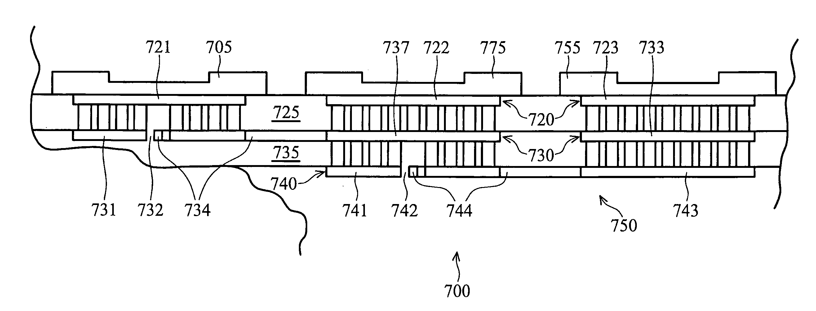
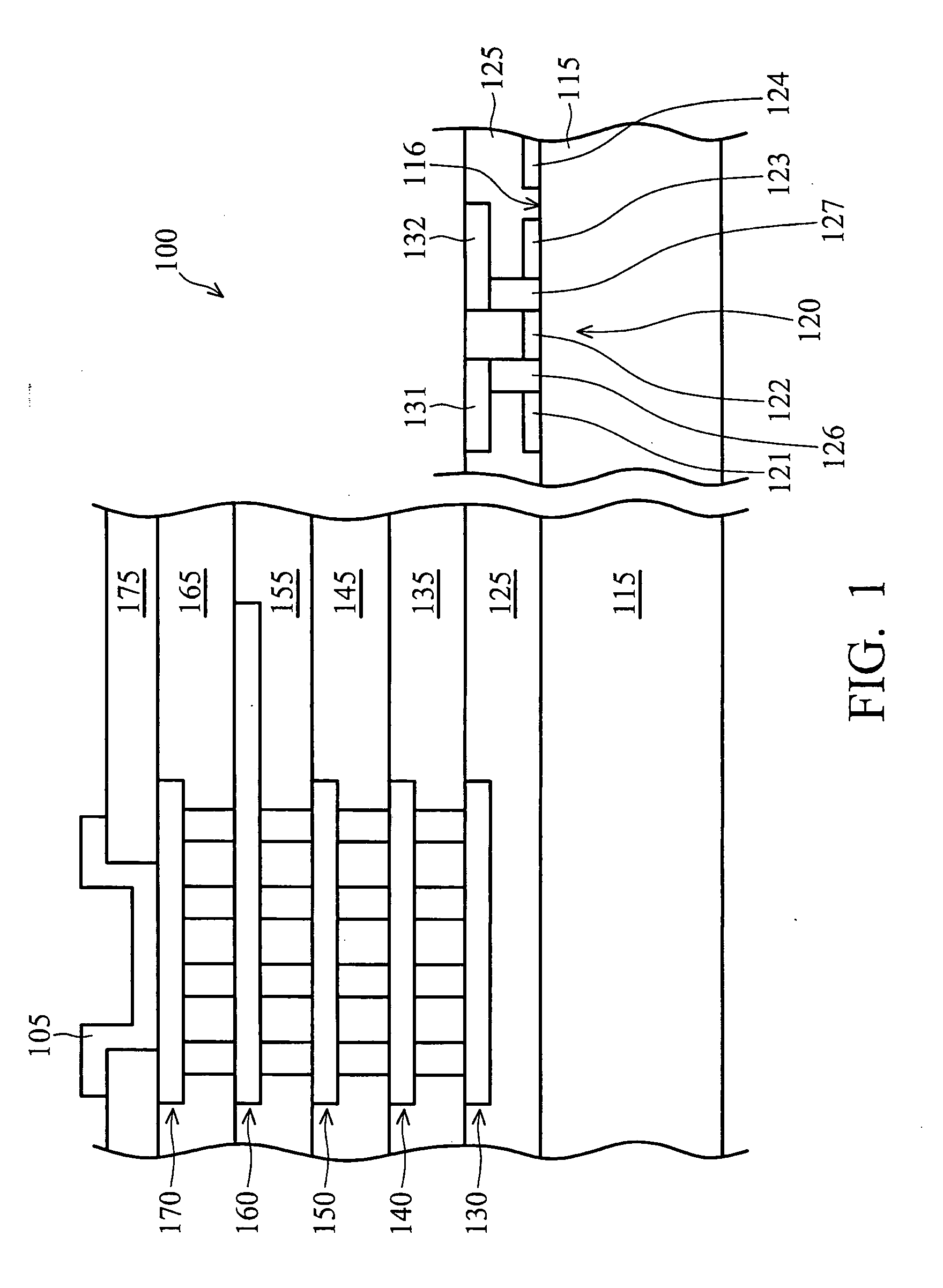
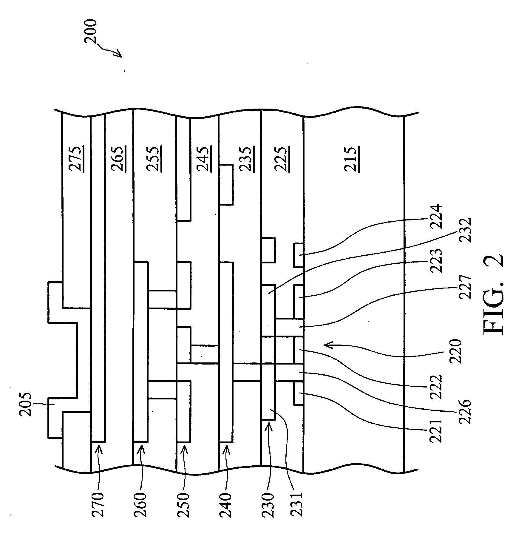
[0027]The present invention will be described with respect to preferred embodiments in a specific context, namely a pad structure for a circuit-under-pad (CUP) flip-chip device. The invention may also be applied, however, to other semiconductor devices as well.

[0028]The present invention is directed to a test structure for use in semiconductor devices. The test structure of the present invention is intended to be integrated into the device, that is, it becomes a part of the semiconductor device itself. Note that the components of the test structure may or may not have other f...


PUM


Abstract

A test structure to detect vertical leakage in a multi-layer flip chip pad stack or similar semiconductor device. The test structure is integrated into the semiconductor device when it is fabricated. A metal layer includes at least two portions that are electrically isolated from each other; one portion being disposed under a test pad, and another portion being disposed under a pad associated with a pad structure being tested. The metal layer in most cases is separated from a top metal layer directly underlying the pads by an inter-metal dielectric (IMD) layer. A metal layer portion underlying the pad to be tested forms a recess in which a conductive member is disposed without making electrical contact. The conductive line is electrically coupled to a test portion of the same or, alternately, of a different metal layer. The test structure may be implemented on multiple layers, with recesses portions underlying the same or different pads.

Description

TECHNICAL FIELD[0001]The present invention relates generally to a field of semiconductor devices, and relates more particularly to a test structure for detecting vertical shorts in a multi-layer semiconductor device associated with a pad for making external connections.BACKGROUND[0002]Generally, semiconductor chips are small pieces of silicon or a similarly-suitable material on which a large number of interconnected electrical devices have been fabricated to form integrated circuits. The circuits are capable of performing a variety of tasks, such as the computations necessary to the operation of personal computers, mobile telephones, and digital cameras. The devices making up the integrated circuits are very small, and there are typically a great number of them on a single chip, which is often less than a square centimeter in area and very thin. Usually, a thin slice of substrate material called a wafer is used as a base for fabricating many chips at the same time, using a number of...

Claims


Application Information

Patent Timeline
IPC IPC(8): H01L23/58
CPCH01L22/32H01L2224/05556H01L2224/05093H01L2224/05096H01L2224/05624H01L2224/05647H01L2924/01013H01L2924/01014H01L2924/01029H01L2924/014H01L24/05H01L2924/01033H01L2924/00014H01L22/34H01L2924/14H01L2924/00
Inventor PENG, TA-CHIHLIN, YU-TINGLIN, LIANG-CHENLEE, KO-YI
Owner TAIWAN SEMICON MFG CO LTD
Why Eureka
Try Eureka