

Epoxy Resin Composition for Semiconductor Encapsulation and Semiconductor Device Using the Same
- Summary
- Abstract
- Description
- Claims
- Application Information
AI Technical Summary
Benefits of technology
Problems solved by technology
Method used
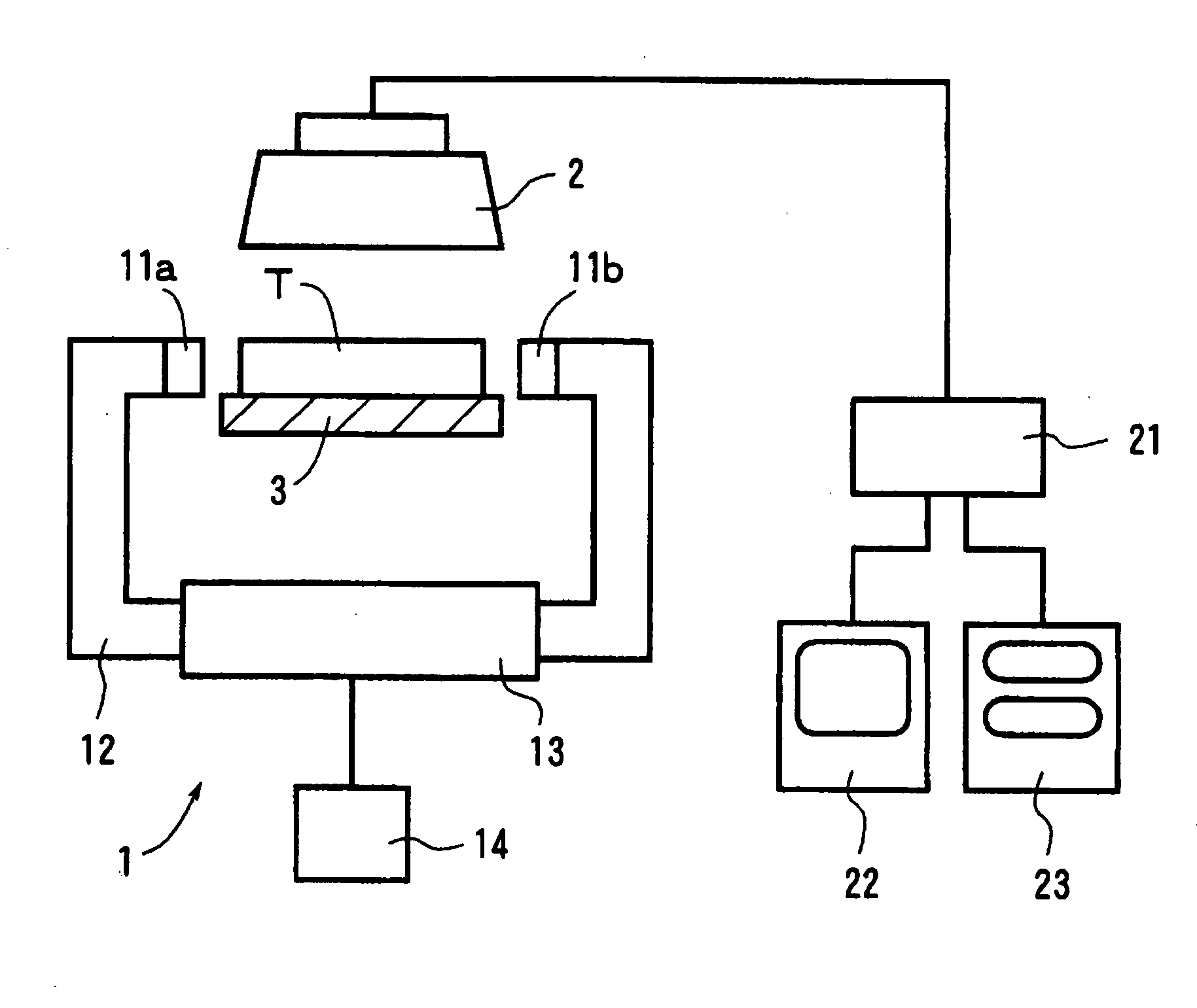
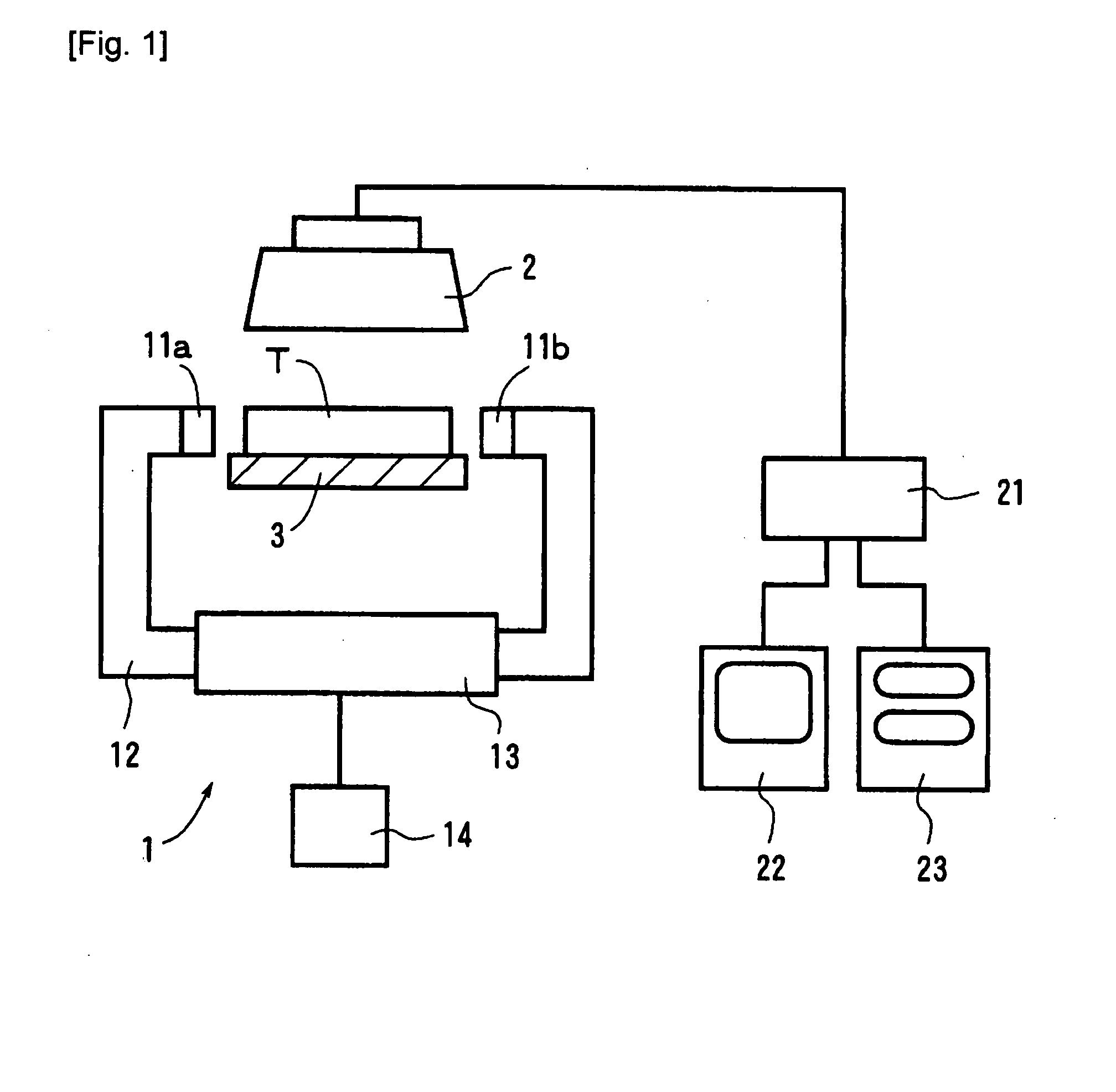
Image

Examples
example 1
Examples 1 and 2, Comparative Examples 1 and 2
[0058]Respective components shown in the following Table 1 were mixed at the ratio shown in the same table and melt-kneaded for 3 minutes using a mixing roller (temperature 100° C.). Next, this melted matter was cooled to room temperature (25° C.) and then pulverized to obtain powder form epoxy resin composition for semiconductor encapsulation. Thereafter, this was processed into a tablet form (diameter 25 mm, thickness 30 mm) using a tablet making machine.
[0059]In the Examples 1 and 2, each of the components was used after detecting and eliminating conductive foreign metallic particles having a size of 20 μm or more in accordance with the conductive foreign metallic particle detection method shown in the following, In addition, as the material of the aforementioned mixing roller, a hard metal having a high.hardness was used, so that the maximum diameter of the foreign particles becomes less than 20 μm even when the material is worn was ...
PUM
| Property | Measurement | Unit |
|---|---|---|
| Length | aaaaa | aaaaa |
| Molar density | aaaaa | aaaaa |
| Fraction | aaaaa | aaaaa |
Abstract
Description
Claims
Application Information