Semiconductor Device Manufacturing Method and Plasma Oxidation Method

a technology of plasma oxidation and semiconductor devices, applied in the direction of coatings, chemical vapor deposition coatings, electric discharge tubes, etc., to achieve the effects of improving the uniformity of oxide film thickness, reducing the variation of film thickness, and improving electrical characteristics

Inactive Publication Date: 2008-06-19
TOKYO ELECTRON LTD
View PDF1 Cites 27 Cited by
  • Summary
  • Abstract
  • Description
  • Claims
  • Application Information

AI Technical Summary

Benefits of technology

[0009]Oxidation using the RLSA microwave plasma can suppress the oxidation of the metal layer, selectively oxidize only the polysilicon layer, and also suppress the formation of a bird's beak. When oxidation is performed using the RLSA microwave plasma, however, the oxide film thickness sometimes varies, so it is still necessary to make this oxide film thickness uniform.
[0063]In addition, the present invention can perform a high density, low electron temperature plasma process by using the RLSA type plasma processing apparatus, thereby decreasing damage to a substrate and forming a high quality oxide film. That is, although the low temperature process is performed, an oxide film on the sidewall of a polysilicon layer is dense and has very high film quality.

Problems solved by technology

Also, oxidation using the RLSA microwave plasma has another problem that since bird's beak formation is excessively suppressed, the edge portion of the polysilicon layer hardly changes its shape and remains as an acute portion, and an electric field concentrates to this acute portion to increase the leakage current.

Method used


Image

  • Semiconductor Device Manufacturing Method and Plasma Oxidation Method
  • Semiconductor Device Manufacturing Method and Plasma Oxidation Method
  • Semiconductor Device Manufacturing Method and Plasma Oxidation Method

Examples


Embodiment Construction

[0092]A preferred embodiment of the present invention will be explained below with reference to the accompanying drawings.

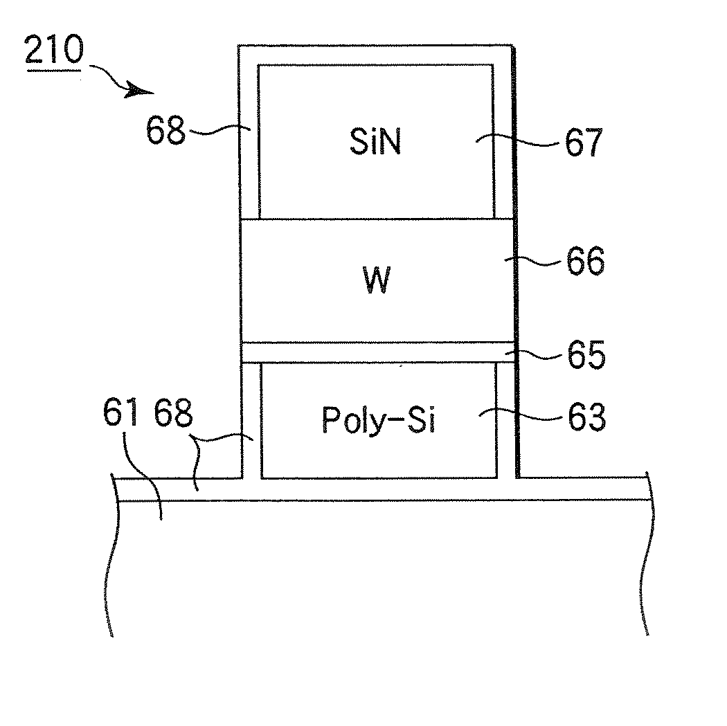
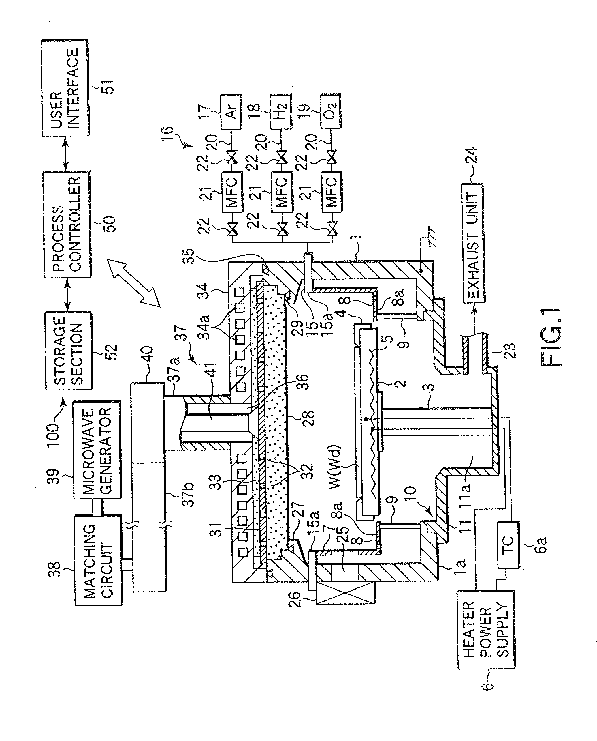
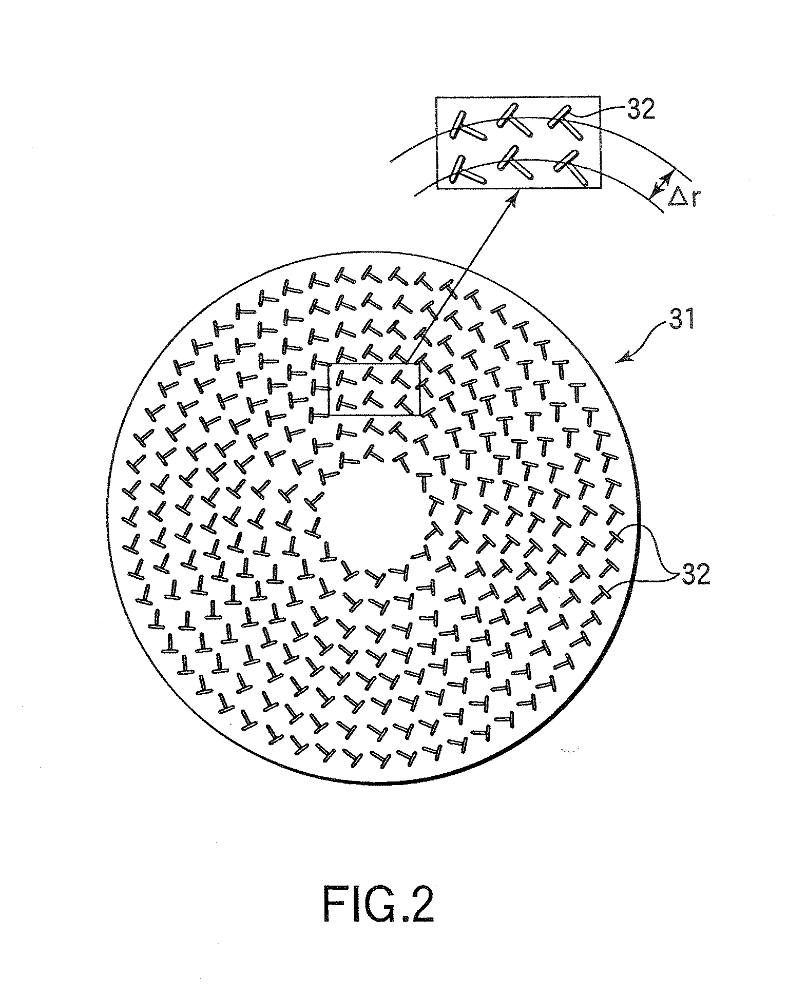
[0093]FIG. 1 is a sectional view schematically showing an example of a plasma processing apparatus suited to practice a plasma oxidation method of the present invention. This plasma processing apparatus is constructed as an RLSA (Radial Line Slot Antenna) microwave plasma processing apparatus capable of generating a high density, low electron temperature microwave plasma by supplying microwaves into a process chamber by using a planar antenna having a plurality of slots, particularly an RLSA, and is suitably used to, e.g., selectively oxidize the sidewalls of polysilicon of a gate electrode.

[0094]A plasma processing apparatus 100 has an almost cylindrical chamber 1 that is airtightly constructed and grounded. A circular opening 10 is formed in an almost central portion of a bottom wall 1a of the chamber 1, and the bottom wall 1a has an exhaust chamber 11 that com...


PUM

PropertyMeasurementUnit
temperatureaaaaaaaaaa
pressureaaaaaaaaaa
flow ratesaaaaaaaaaa

Abstract

A semiconductor device manufacturing method includes forming a gate insulating film on a semiconductor substrate; forming, on the gate insulating film, a multilayered structure including at least a polysilicon layer and a metal layer containing a refractory metal; forming a gate electrode by etching the multilayered structure; and performing a plasma process by a plasma processing apparatus, which is configured to supply microwaves into a process chamber from a planar antenna including a plurality of slots and thereby to generate plasma, at a process pressure of 133.3 to 1,333 Pa and a process temperature of 250 to 800° C. by using a process gas containing at least hydrogen gas and oxygen gas, thereby selectively oxidizing the polysilicon layer in the gate electrode.

Description

TECHNICAL FIELD[0001]The present invention relates to a semiconductor device manufacturing method and plasma oxidation method including a step of processing a semiconductor substrate by use of plasma.BACKGROUND ART[0002]Recently, the design rules of semiconductor elements forming LSIs are still more miniaturized in order to meet demands for a high integration degree and high speed of LSIs. Accordingly, a demand has arisen for decreasing the resistance of the gate electrode of a transistor used in a DRAM or flash memory. Although polysilicon is conventionally used as the gate electrode, polysilicon has the drawback that the sheet resistance is high. Therefore, as a metal having a low resistance value, high adhesion to a silicon oxide film and silicon itself, and high processability, it has been proposed to stack a refractory metal such as tungsten or its silicide on a polysilicon layer. More specifically, tungsten polycide (a stacked film of WSi / poly-Si) and a tungsten poly-metal gat...

Claims


Application Information

Patent Timeline
Patent Type & Authority Applications(United States)
IPC IPC(8): H01L21/31C23C16/00
CPCH01J37/32192H01J37/32935H01L21/32105H01L21/28247H01L21/28061H01L29/4941
Inventor SASAKI, MASARU
Owner TOKYO ELECTRON LTD
Why Eureka
Try Eureka