Plastic electronic component package

a technology of electronic components and plastics, applied in the direction of transportation and packaging, basic electric elements, mechanical equipment, etc., can solve the problems of difficult to accurately align the glass cover to the ceramic frame, the ceramic package is expensive, and the ceramic package is not readily adapted to strip or other multiple unit manufacturing,

Inactive Publication Date: 2008-06-26
IQLP
View PDF22 Cites 32 Cited by
  • Summary
  • Abstract
  • Description
  • Claims
  • Application Information

AI Technical Summary

Benefits of technology

[0007]The image sensor package according to the present invention eliminates the need for ceramic components and employs a plastic material which preferably is a high temperature liquid crystal polymer (LCP) material. The package is useful not only for image sensors but also for other light sensing or light emitting semiconductor or other devices or components. A package in accordance with the invention can also be used to contain non-optical devices or components.

Problems solved by technology

The ceramic package is expensive and not readily adapted to manufacture in strip form or other multiple unit form, as is widely employed in the semiconductor packaging industry.
In addition, the use of epoxy as a bonding agent presents several problems such as moisture penetration through the epoxy bond, outgassing of the epoxy which can contaminate the semiconductor device, and air leakage which limits the ability to hermetically seal the ceramic package.
Further, it is difficult to accurately align the glass cover to the ceramic frame so that the glass cover is parallel to the image sensor surface.
This alignment difficulty is caused by an inability to control the thickness of an epoxy bead which is commonly employed to seal the glass lid to the ceramic frame.
The requirement for UV curable adhesive materials limits the range of available epoxies which can be employed in the conventional ceramic package, since most epoxy adhesives are curable at elevated temperatures.
Moisture or corrosive gases on or near a semiconductor device can cause corrosion of the metallic traces on the semiconductor device, and can lead to failure.
These materials have such low permeabilities that moisture and fluids typically are impeded by these materials, and cause a condensation on the semiconductor device or contamination by corrosive gasses.

Method used


Image

  • Plastic electronic component package
  • Plastic electronic component package
  • Plastic electronic component package

Examples


Embodiment Construction

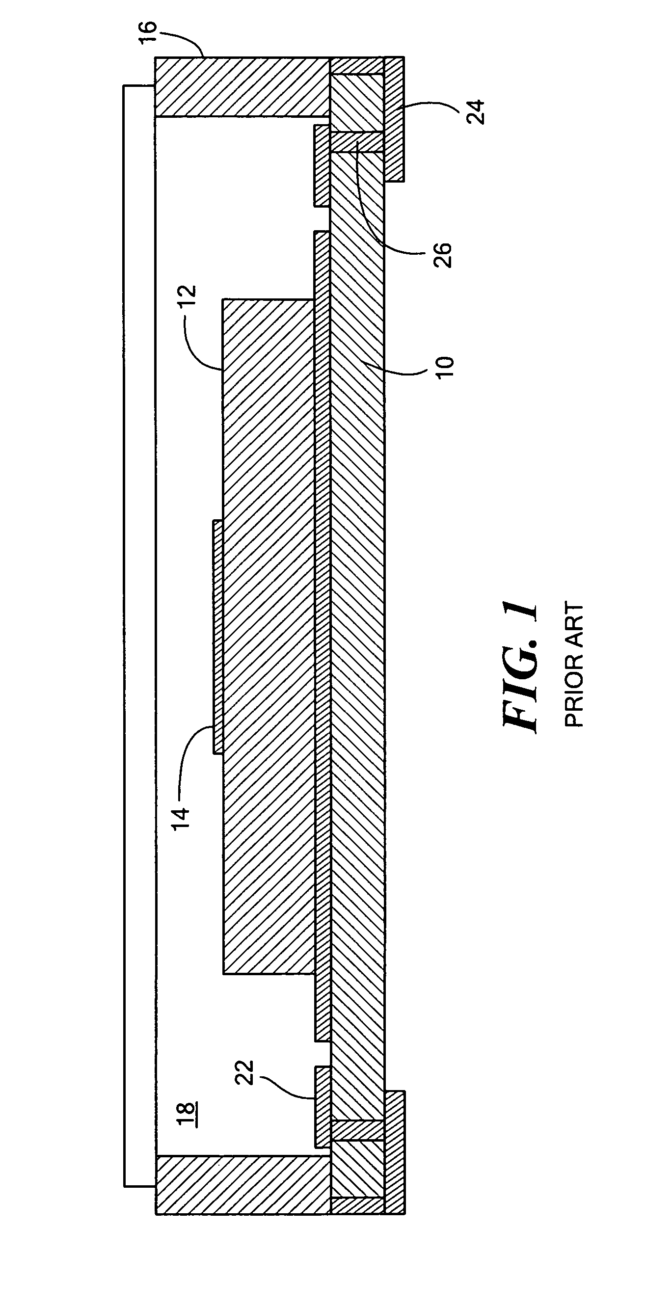
[0027]The package, materials and method of package fabrication are described in a preferred embodiment for an image sensor. The invention is not to be limited to image sensor packages or packages for other optical devices, but is more broadly useful for housing other semiconductor, electrical and electronic devices, components or circuits.

[0028]The package configuration can be of various forms to suit particular packaging requirements. The package configuration may vary in size and shape and can include electrical lead configurations of many different forms. The invention is not to be limited to any particular package type or configuration. The invention will be described in the context of a package for a semiconductor image sensor chip such as used in digital cameras and other digital imaging systems and devices.

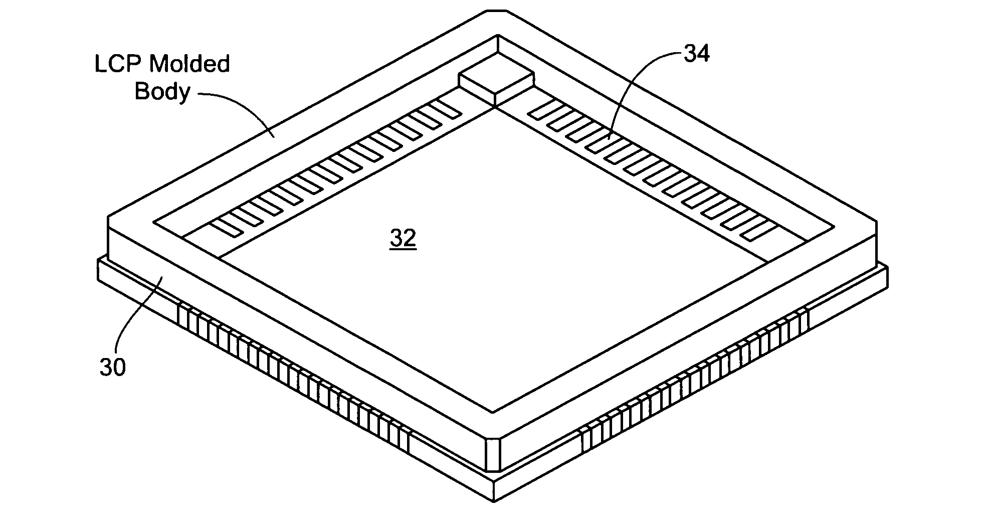
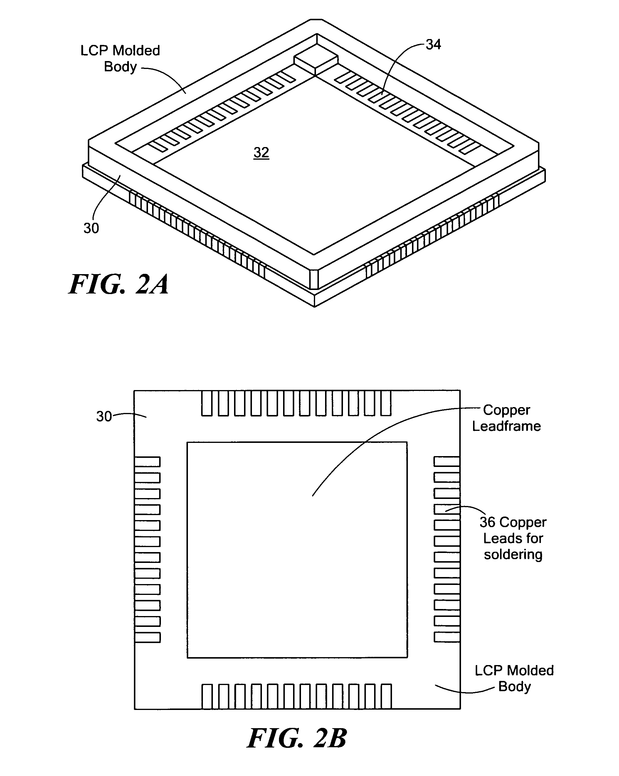
[0029]The image sensor package in accordance with the invention comprises a high temperature thermoplastic body or frame, preferably an LCP material, molded around a metal ...


PUM

PropertyMeasurementUnit
melting temperatureaaaaaaaaaa
particle sizeaaaaaaaaaa

Abstract

A plastic package for an image sensor or other electronic component which comprises a plastic body, preferably of LCP material, molded around a leadframe and defining a cavity in which the image sensor is to be disposed. A lid assembly is provided having a transparent glass lid retained in a plastic lid frame which is weldable or otherwise bondable to the plastic body of the package to enclose the image sensor mounted in the cavity. The leadframe is usually composed of copper or a copper alloy, or a ferrous alloy having a copper coating. An interfacial layer is formed on the surfaces of the leadframe at least in those portions which are in contact with the plastic body which serves to provide substantially improved adhesion between the leadframe and the plastic material to achieve a hermetic bond between the metal and plastic materials. The interfacial layer is composed of a cuprous oxide base layer formed on a surface of the leadframe, and a cupric oxide layer formed on the cuprous oxide layer. The cupric oxide outer layer has an acicular structure which provides an interlocking mechanism for adhesion to the plastic material molded thereto in forming the package.

Description

CROSS REFERENCE TO RELATED APPLICATIONS[0001]This application claims the benefit under 35 U.S.C. §119(e) of U.S. Provisional Patent Application No. 60 / 874,450, filed on Dec. 12, 2006, the disclosure of which is incorporated by reference herein.STATEMENT REGARDING FEDERALLY SPONSORED RESEARCH OR DEVELOPMENT[0002]N / ABACKGROUND OF THE INVENTION[0003]Image sensors such as those used in digital cameras and other optical or image sensing equipment are conventionally housed in a ceramic package. The ceramic package includes a ceramic frame which is epoxy bonded to a glass lid or cover. The ceramic package is expensive and not readily adapted to manufacture in strip form or other multiple unit form, as is widely employed in the semiconductor packaging industry. In addition, the use of epoxy as a bonding agent presents several problems such as moisture penetration through the epoxy bond, outgassing of the epoxy which can contaminate the semiconductor device, and air leakage which limits the ...

Claims


Application Information

Patent Timeline
Patent Type & Authority Applications(United States)
IPC IPC(8): H01L31/0203H01L23/495H01L21/60
CPCH01L23/10Y10T428/12569H01L23/49861H01L27/14618H01L27/14683H01L33/486H01L2224/48227H01L2224/4899H01L2924/01012H01L2924/0102H01L2924/01078H01L2924/01079H01L2924/09701H01L2924/3025H01L24/48H01L2224/48091H01L23/3142Y10T428/12618H01L2924/12041H01L2924/00014H01L2924/00H01L2924/15747H01L2924/16195H01L2924/181Y10T428/31678H01L2224/45099H01L2224/45015H01L2924/207
Inventor ZIMMERMAN, MICHAEL A.SMITH, KEITHSHVERDIN, JACOB
Owner IQLP
Why Eureka
Try Eureka