Selective processing of semiconductor nanowires by polarized visible radiation

a visible radiation and selective processing technology, applied in nanoinformatics, ohmic resistance heating, manufacturing tools, etc., can solve the problems of damage to the crystalline lattice of nanowires, the inability to accurately align and position the appropriately doped regions of nanowires to build functional devices using currently known assembly techniques, and the inability to accurately align and position the appropriately doped regions of nanowires

Active Publication Date: 2008-06-26
ONED MATERIAL LLC +1
View PDF53 Cites 45 Cited by
  • Summary
  • Abstract
  • Description
  • Claims
  • Application Information

AI Technical Summary

Benefits of technology

[0011]Methods, systems, and apparatuses for processing semiconductor nanowires are provided. Laser annealing is used to process nanowires. For example, the laser annealing may be used to activate dopants in the nanowires, and/or to repair damag...

Problems solved by technology

Even though modulation of doping profiles along the length of nanowires can be achieved, accurate alignment and positioning of the appropriately doped regions of the nanowires to build functional devices using currently known assembly techniques can be extremely cumbersome.
Furthermore, different types of nanowire semiconducting materials can suffer from further problems.
H...

Method used


Image

  • Selective processing of semiconductor nanowires by polarized visible radiation
  • Selective processing of semiconductor nanowires by polarized visible radiation
  • Selective processing of semiconductor nanowires by polarized visible radiation

Examples


case b

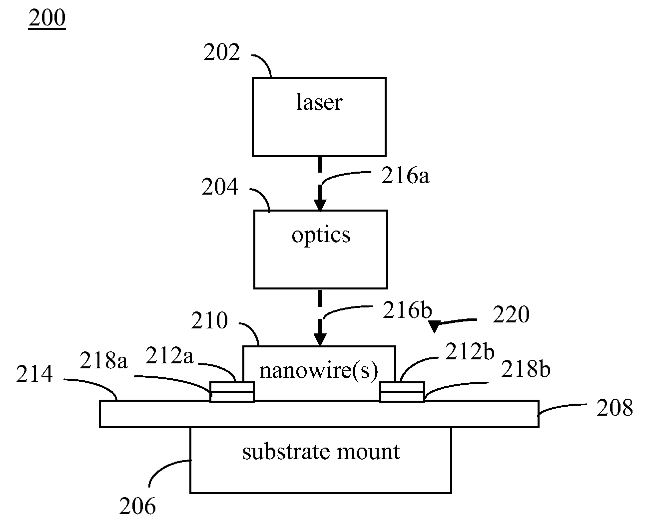
[0108]In case B, relative to case A, larger fluences are required to anneal and / or damage the silicon nanowires. In both of cases A and B, a threshold fluence for nanowire damage is lower than reported threshold values for melting silicon thin films and bulk silicon, which are typically hundreds of millijoules per square centimeter. This may be due to a strong absorption efficiency of nanowires, and small heat losses to the ambient environment and due to a thermal conductance to the substrate. The latter attribute may be responsible for a prolonged cooling cycle, thereby allowing the nanowires to reside longer at an elevated temperature, facilitating an efficient annealing process. Assuming bulk silicon thermal properties, at a fluence level of approximately 30 mJ / cm2 for a 30 nm wire with an absorption efficiency of 0.1, a temperature rise of about 790 K is predicted if all the absorbed energy were to heat the nanowire. Such an estimate would predict a linear dependence on the ...


PUM

PropertyMeasurementUnit
Surface energyaaaaaaaaaa
Flexibilityaaaaaaaaaa

Abstract

Methods, systems, and apparatuses for annealing semiconductor nanowires and for fabricating electrical devices are provided. Nanowires are deposited on a substrate. A plurality of electrodes is formed. The nanowires are in electrical contact with the plurality of electrodes. The nanowires are doped. A polarized laser beam is applied to the nanowires to anneal at least a portion of the nanowires. The nanowires may be aligned substantially parallel to an axis. The laser beam may be polarized in various ways to modify absorption of radiation of the applied laser beam by the nanowires. For example, the laser beam may be polarized in a direction substantially parallel to the axis or substantially perpendicular to the axis to enable different nanowire absorption profiles.

Description

[0001]This application claims the benefit of U.S. Provisional Application No. 60 / 872,015, filed on Nov. 29, 2006, which is incorporated by reference herein in its entirety.STATEMENT REGARDING FEDERALLY SPONSORED RESEARCH OR DEVELOPMENT[0002]This invention was made with government support under Contract No. W31P4Q-05-C—R193 awarded by the United States Army Aviation and Missile Command (c / o DARPA). The government has certain rights in the invention.BACKGROUND OF THE INVENTION[0003]1. Field of the Invention[0004]The present invention relates to the processing of semiconductor nanowires.[0005]2. Background of the Invention[0006]Nanowires are drawing tremendous interest due to their unique properties like high surface to volume ratio and dimensionality. Controlled nanowire growth methods can reliably synthesize nanowires of varying composition and size. Furthermore, advances in nanowire assembly techniques have enabled devices based on nanowires to be realized. Semiconductor nanowires m...

Claims


Application Information

Patent Timeline
IPC IPC(8): H01L23/48H01L21/44H01L21/02H05B1/00
CPCB23K26/073B82Y10/00H01L21/26513H01L21/268H01L29/0665H01L2924/0002H01L29/0673H01L29/78H01L2924/00H01L21/2658
Inventor STUMBO, DAVID P.PAN, YAOLINGGRIGOROPOULOS, COSTAS P.MISRA, NIPUN
Owner ONED MATERIAL LLC
Why Eureka
Try Eureka