Method for manufacturing thin film transistor

a thin film transistor and manufacturing method technology, applied in the direction of electrical equipment, semiconductor devices, instruments, etc., can solve the problems of unsolved exposure processes in use for a considerable time, the enlargement of the tft component area, and the inability to obtain the desired pattern in the large-scale panel. , to achieve the effect of increasing the ion current of the tft, reducing the l-shaped channel length of the tft, and relatively reducing the l-shaped

Active Publication Date: 2008-07-03
AU OPTRONICS CORP
View PDF5 Cites 12 Cited by
  • Summary
  • Abstract
  • Description
  • Claims
  • Application Information

AI Technical Summary

Benefits of technology

[0008]In the present invention, a source, a drain, and a channel therebetween are defined and formed through two lithographic process cycles. Therefore, the channel length (L) of the thin film transistor (TFT) can be reduced so as to increase the Ion current of the TFT. Moreover, the component area of the TFT is relatively decreased as the channel width (W) is decreased. Thus, the aperture ratio of the TFT-LCD can be increased due to the decreased component area of the thin film transistor.

Problems solved by technology

Nevertheless, if the source / drain (S / D) is designed in U-type or double-U-type, it still enlarges the area of the TFT component.
Additionally, the desired pattern can not be obtained in the large-sized panel through being exposed by only one mask.
The aforementioned problems of the exposure processes in use have remained unsolved for some considerable time.

Method used


Image

  • Method for manufacturing thin film transistor
  • Method for manufacturing thin film transistor
  • Method for manufacturing thin film transistor

Examples


embodiment 1

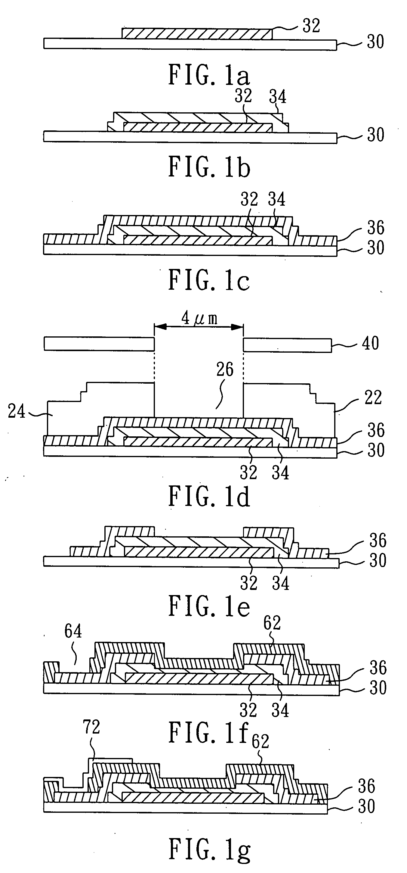
[0053]With reference to FIGS. 2a to 2h, there is shown a flowchart in a perspective view of the method in Embodiment 1 of the present invention.

[0054]As shown in FIG. 2a, first, a substrate 30 is provided. The substrate 30 can be a glass substrate, a quartz substrate, or a plastic substrate. Subsequently, in a step of forming a first pattern, a patterned first metal layer 32, as a gate of the TFT, is formed on the substrate 30. The first metal layer can be made of Al, W, Cr, Cu, Ti, TiNx, Al alloy, Cr alloy, or Mo, and it can be a single-layered structure, or a multiple-layered structure.

[0055]As shown in FIG. 2b, a step of forming a second pattern is performed. A patterned semiconductor layer 34 is formed on the patterned first metal layer 32, especially covering the patterned first metal layer 32 for example. The patterned semiconductor layer 34 can be made of amorphous silicon (α-Si).

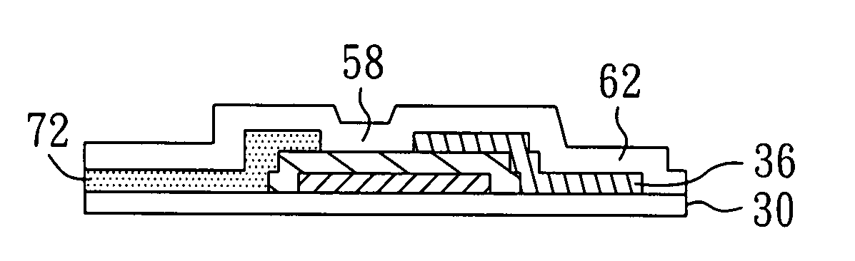
[0056]As shown in FIG. 2c, a second metal layer 36 is formed on the patterned semiconductor layer...

embodiment 2

[0065]With reference to FIG. 3a to FIG. 3h, there is shown a flowchart in a perspective view of the method in Embodiment 2 of the present invention. The processes in the present embodiment basically are similar to those in aforementioned Embodiment 1, and the differences therebetween are illustrated hereinafter.

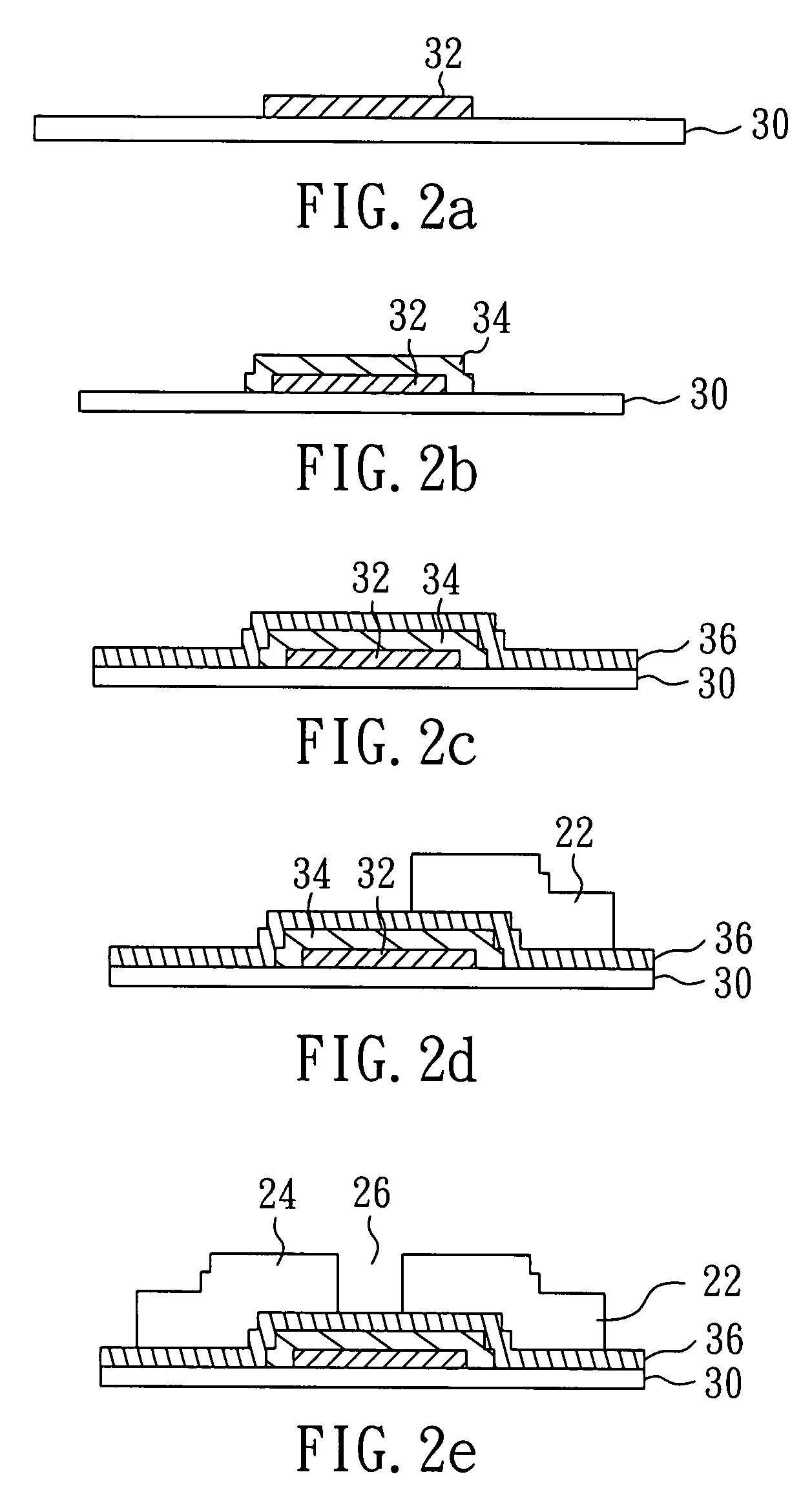
[0066]As shown in FIG. 3a, first, a substrate 30 is provided. The substrate 30 can be a glass substrate, a quartz substrate, or a plastic substrate. Subsequently, in a step of forming a first pattern, a patterned first metal layer 32, as a gate of the TFT, is formed on the substrate 30. The first metal layer can be made of Al, W, Cr, Cu, Ti, TiNx, Al alloy, Cr alloy, or Mo, and it can be a single-layered structure, or a multiple-layered structure.

[0067]As shown in FIG. 3b, an insulation layer 31, a semiconductor layer 34, an ohm contact layer 33, and a second metal layer 36 are formed in sequence on the patterned first metal layer 32. The insulation layer 31 can be made of Si...

embodiment 3

[0076]With reference to FIG. 4a to FIG. 4i, there is shown a flowchart in a perspective view of the method in Embodiment 3 of the present invention. The processes in the present embodiment basically are similar to those in aforementioned Embodiment 1, and the differences therebetween are illustrated hereinafter.

[0077]As shown in FIG. 4a, first, a substrate 30 is provided. The substrate 30 can be a glass substrate, a quartz substrate, or a plastic substrate. Subsequently, in a step of forming a first pattern, a patterned first metal layer 32, as a gate of the TFT, is formed on the substrate 30. The first metal layer can be made of Al, W, Cr, Cu, Ti, TiNx, Al alloy, Cr alloy, or Mo, and it can be a single-layered structure, or a multiple-layered structure.

[0078]As shown in FIG. 4b, a step of forming a second pattern is performed. A patterned semiconductor layer 34 is formed on the patterned first metal layer 32. The patterned semiconductor layer 34 can be made of amorphous silicon (α-...


PUM


Abstract

A method for manufacturing a thin film transistor (TFT) is disclosed. The method is achieved by forming and defining a source and a drain of a thin film transistor through two lithographic processes cycles so that the channel length (L) of the thin film transistor can be reduced to 1.5 to 4.0 μm. Besides, the Ion current of the thin film transistor is increased as the channel length (L) is decreased. Therefore, the component area of the thin film transistor is decreased as the channel width (W) is decreased. Thus, the aperture ratio of the TFT-LCD can be increased due to the decreased component area of the thin film transistor.

Description

BACKGROUND OF THE INVENTION[0001]1. Field of the Invention[0002]The present invention relates to a method for manufacturing a thin film transistor and, more particularly, to a method for manufacturing a thin film transistor used for a large-sized display device.[0003]2. Description of Related Art[0004]Generally, a thin film transistor liquid crystal display device (TFT-LCD) mainly consists of a TFT array substrate, a color filter array substrate, and a liquid crystal (LC) layer, wherein the TFT array substrate includes plural pixel structures that consist of plural transistors in array arrangement and plural pixel electrodes. Each of the pixel electrodes corresponds to every transistor. The above-mentioned TFT mainly comprises a gate, a semiconductor layer, a source, a drain, and a channel. Mostly, the TFT is a switch component adopted for a liquid crystal display pixel unit.[0005]Currently, the development object of LCDs tends toward a large size, high brightness, high contrast, a ...

Claims


Application Information

Patent Timeline
Patent Type & Authority Applications(United States)
IPC IPC(8): H01L27/12H01L21/336
CPCH01L29/66757H01L27/1214H01L27/1288G02F1/13439H01L27/124H01L29/458H01L29/78696
Inventor LIU, CHANG-WEI
Owner AU OPTRONICS CORP
Why Eureka
Try Eureka