Structure and method for mobility enhanced mosfets with unalloyed silicide

a technology of enhanced mobility and silicide, which is applied in the direction of semiconductors, electrical devices, semiconductor devices, etc., can solve the problems of similar problems encountered with silicon substitutional alloys, the general complexity of such processes remains a challenge, and the successful implementation of pfets and nfets with enhanced mobility through stress engineering on the same silicon substrate requires a complex integration of processing steps

Active Publication Date: 2008-07-10
AURIGA INNOVATIONS INC
View PDF7 Cites 49 Cited by
  • Summary
  • Abstract
  • Description
  • Claims
  • Application Information

AI Technical Summary

Benefits of technology

[0037]The second group of embodiments provides unalloyed silicide only over the silicon germanium alloy but not over the Si:C alloy. As with the first group of embodiments, the second group of embodiments also increases the height of the source and the drain, as defined by the interface between the contact material and the semiconductor material, significantly higher than an equivalent structure that does not utilize a selective silicon deposition during the process flow. However, since all the material deposited by selective silicon deposition turned into silicon carbon alloy under the second variety of surfaces, given the same thickness for the newly grown silicon layer, the amount of silicon carbon alloy above the gate dielectric is more according to the second group of embodiments than the corresponding amount according to the first group of embodiments. Hence, the stress enhancement is more on devices with embedded silicon carbon alloy according to the second group of embodiments.

Problems solved by technology

Similar problems are encountered with substitutional alloys of silicon and germanium.
While the second approach does produce devices with improved performance, such an approach faces some challenges in that the formation of a crystalline structure with an altered lattice parameter generally depends on the structural relaxation of the epitaxially grown alloy material, be it an alloy of silicon and germanium or an alloy of silicon and carbon, through the generation of misfit dislocations, which are crystalline defects in thick films.
Manufacturing both PFETs and NFETs with enhanced mobility through stress engineering on the same substrate, therefore, creates a challenge in that two types of substrate areas with an altered lattice parameter need to be fabricated.
However, the general complexity of such processes still remains a challenge.
As in the case of the second approach discussed above, a successful implementation of both PFETs and NFETs with enhanced mobility through stress engineering on the same silicon substrate requires a complex integration of processing steps.
The first problem is a degradation of contact resistance on SiGe alloy.
As the content of germanium increases, the contact resistance to the source and drain also tends to increase and degrade the performance of PFETs with embedded SiGe alloy in the source and the drain.
This is because the alloy of metal silicide and metal germanide, which is formed by depositing a metal on the source and drain containing silicon and germanium and annealing the structure during the contact formation process, has inferior contact resistance to unalloyed metal silicide, that is, a metal silicide without any metal germanide mixed within.
Metal silicides formed upon such surfaces have degraded performance compared to normal silicide formed on flat surface containing no carbon.
Furthermore, it has been discovered that not only the reaction rate of the Si:C selective epitaxy process is very slow, but there is also a limit on the thickness of the Si:C films that can be grown by selective epitaxy process currently available in the industry.
This means that the increase in the height of the source and the drain through the use of Si:C selective epitaxy has a limit, and that Si:C selective epitaxy is not conducive to manufacturing of NFET structures with highly raised source and drain relative to the height of the gate dielectric.

Method used


Image

  • Structure and method for mobility enhanced mosfets with unalloyed silicide
  • Structure and method for mobility enhanced mosfets with unalloyed silicide
  • Structure and method for mobility enhanced mosfets with unalloyed silicide

Examples


first embodiment

[0058]The present invention may also be presented in at least twelve different embodiments. All of these embodiments share some common processes and features. Therefore, the present invention is described in detail for the first embodiment, although other embodiments may also be demonstratively illustrated in the various drawings. Thereafter, differences among different embodiments of the present invention are compared and described.

[0059]In typical CMOS processing, some areas of the surface of the semiconductor substrate are used for building PFET structures. These areas are collectively called “the PFET area” herein. Similarly, some other areas of the surface of the semiconductor substrate are used for building NFET structures. They are collectively called “the NFET area” herein. An exemplary PFET structure in the PFET area and an exemplary NFET structure in the NFET area at various stages of the manufacturing sequences are described for the description of the present invention he...

seventh embodiment

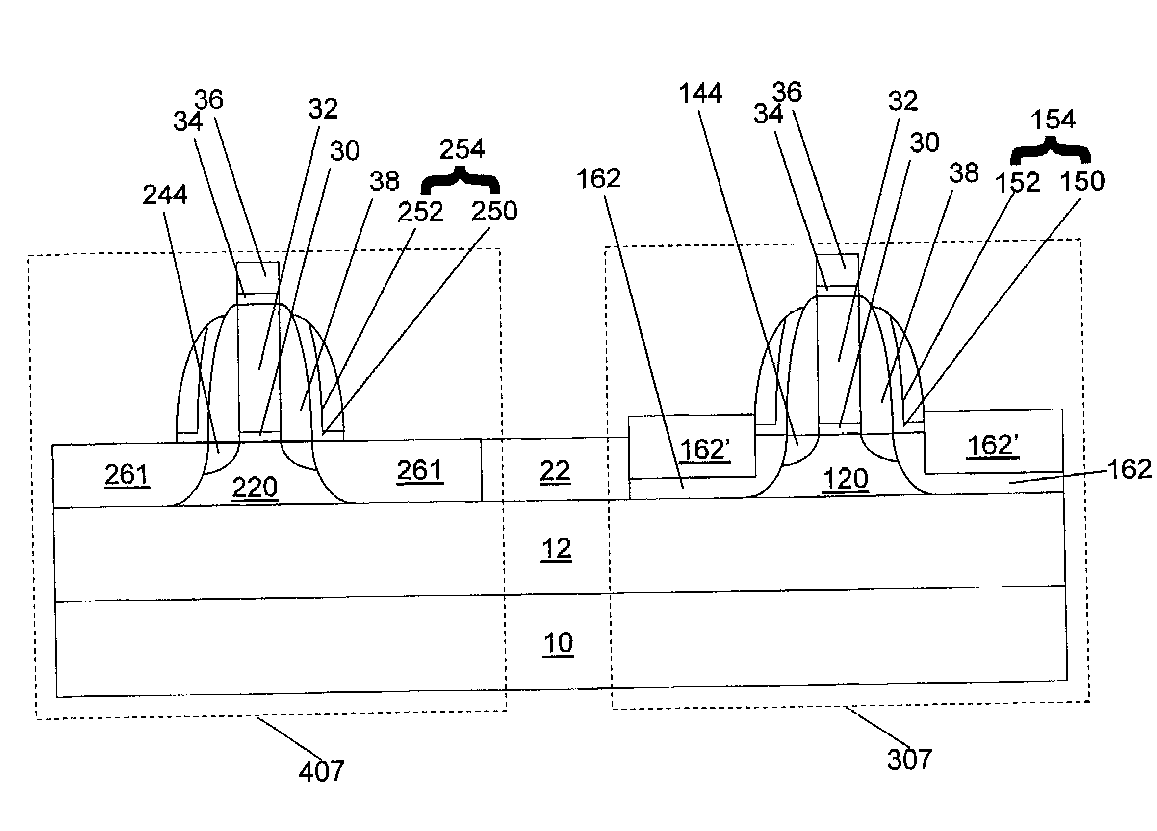
[0098]According to the present invention, the reaction of the metal 80 is controlled such that the contact formation process consumes only a portion of the N-doped Si:C alloy layer 872′ and the P-doped silicon layer. A PFET structure 711 and an NFET structure 811 at this stage is shown in FIG. 20. The body of the PFET 120, the PFET extension 144, the P-doped silicon 762, the P-doped silicon germanium alloy 762′, and the unreacted P-doped silicon layer 772 form a contiguous single crystalline structure within each area surrounded by STI 22. Likewise, the body of the NFET 220, the NFET extension 244, the N-doped silicon 862, the N-doped Si:C alloy 862′, and the unreacted N-doped silicon layer 874′ form a contiguous single crystalline structure within each area surrounded by STI 22.

[0099]According to the eighth embodiment of the present invention, the reaction of the metal 80 is controlled such that the contact formation process consumes all of the N-doped Si:C alloy layer 872′ and the...


PUM

PropertyMeasurementUnit
temperatureaaaaaaaaaa
lattice constantsaaaaaaaaaa

Abstract

While embedded silicon germanium alloy and silicon carbon alloy provide many useful applications, especially for enhancing the mobility of MOSFETs through stress engineering, formation of alloyed silicide on these surfaces degrades device performance. The present invention provides structures and methods for providing unalloyed silicide on such silicon alloy surfaces placed on semiconductor substrates. This enables the formation of low resistance contacts for both mobility enhanced PFETs with embedded SiGe and mobility enhanced NFETs with embedded Si:C on the same semiconductor substrate. Furthermore, this invention provides methods for thick epitaxial silicon alloy, especially thick epitaxial Si:C alloy, above the level of the gate dielectric to increase the stress on the channel on the transistor devices.

Description

FIELD OF THE INVENTION[0001]The present invention relates to semiconductor devices and methods of manufacture, and particularly, to complementary metal oxide semiconductor (CMOS) transistors with stress in the channels.BACKGROUND OF THE INVENTION[0002]Each new generation of semiconductor technology demands higher performance in semiconductor devices, particularly in the performance of CMOS transistors. One of the key metrics of transistor performance is the on-current of the transistor per unit width, typically measured in hundreds of microamperes per micron of the channel width, or “gate width” as it is commonly referred to. Various methods have been considered and practiced to enhance the on-current of the CMOS transistors, that is, both PFETs (transistors wherein the minority carriers are holes, which are p-type carriers), and NFETs (transistors wherein the minority carriers are electrons, which are n-type carriers). Among them, improving the mobility of minority carriers in the ...

Claims


Application Information

Patent Timeline
Patent Type & Authority Applications(United States)
IPC IPC(8): H01L27/092H01L21/8238
CPCH01L21/823807H01L21/823814H01L21/823864H01L21/84H01L27/1203H01L29/165H01L27/3279H01L29/6656H01L29/66628H01L29/66636H01L29/7848H01L21/76886H01L29/665H01L21/8238H10K59/1315
Inventor LIU, YAOCHENGCHIDAMBARRAO, DURESETIGLUSCHENKOV, OLEGHOLT, JUDSON R.MO, RENEE T.RIM, KERN
Owner AURIGA INNOVATIONS INC
Why Eureka
Try Eureka