Repairing integrated circuit memory arrays

a technology of memory arrays and integrated circuits, which is applied in the direction of read-only memories, instruments, and static storage, etc., can solve the problems of inability to repair then, inability to provide redundant columns and rows, and inability to use integrated circuits, etc., to achieve the effect of simplifying the repair control circuitry, increasing read speed, and reducing write speed

Active Publication Date: 2008-07-10
ARM LTD
View PDF4 Cites 4 Cited by
  • Summary
  • Abstract
  • Description
  • Claims
  • Application Information

AI Technical Summary

Benefits of technology

[0019]Within the context of integrated circuits containing a plurality of arrays of memory cells, an array select signal can be used to control the repair control circuitry to select one of the plurality of arrays of memory cells to operated in the repair mode. A single array requiring repair by operating in the repair mode is statistically the most likely occurrence and accordingly simplifying the repair control circuitry to operating in this manner represents a good trade off between complexity and usefulness.
[0020]It will be appreciated that when operating in the repair mode whilst sharing memory cells to drive values out onto the bit lines may increase read speed, the need to write into more than one memory cell during a write could reduce write speed and accordingly it is desirable to provide a write signal driver of increased strength and of at least sufficient strength to write to the number of memory cells which act together in the repair mode.
[0021]The same issue can also be addressed by providing timing and control circuitry able to extend the write cycle time and potentially reduce the read cycle time.

Problems solved by technology

Whilst these techniques are effective in improving the yield of useable integrated circuits, they suffer from the disadvantage of requiring additional circuit area overhead to provide the redundant columns and rows.
Furthermore, a finite number such redundant columns may be provided and, if the number of defective rows or columns exceeds the number of redundant rows or columns, then repair then cannot be made and the integrated circuit cannot be used.
As process geometry is falling in size, the vulnerability of circuit elements within memory arrays to defects in their manufacture increases.
Furthermore, the bit cell “on” current is not increasing in line with the historical scaling trends due to many reasons, including scaling limitations of gate oxide and threshold voltage.
In addition, the increased significance of two dimensional electric field effects and other effects relating to the physics of operation of small scale circuit elements further increase the “off” current due to phenomenon such as gate tunneling and band-to-band tunneling which make the ratio of the on-to-off current even worse.
As a consequence of the above factors, a bit cell being read might not be able to provide sufficient current for the bit line pair to develop a sufficient voltage differential during the time period required for sensing the stored data value.
This would result in either an error in the state being read or the speed requirements for the memory not being met.
It should be noted that the traditional redundancy schemes, and particularly redundant rows, have a significant area and timing overhead.
In addition, they are ill suited to repairing for drifts in process parameters, weak or erratic bits or defects of a gross nature.
However, as the process scales to smaller geometries, acceptable levels of margin in the design still result in a significant number of integrated circuits being produced which have errors beyond those which can be repaired by traditional row and column redundancy techniques.
This problem is likely to become more severe as the geometries scale to smaller sizes.

Method used


Image

  • Repairing integrated circuit memory arrays
  • Repairing integrated circuit memory arrays
  • Repairing integrated circuit memory arrays

Examples


Embodiment Construction

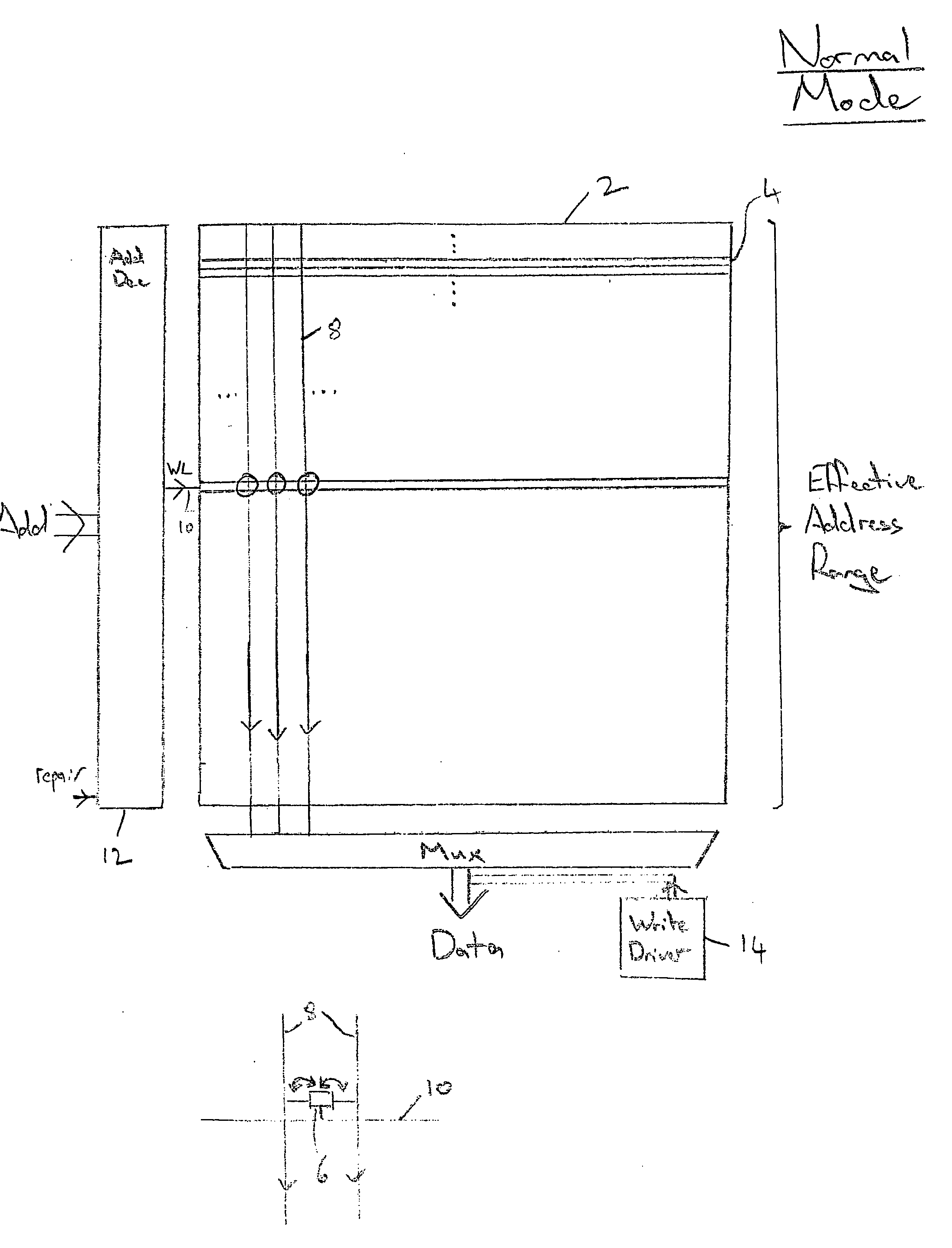
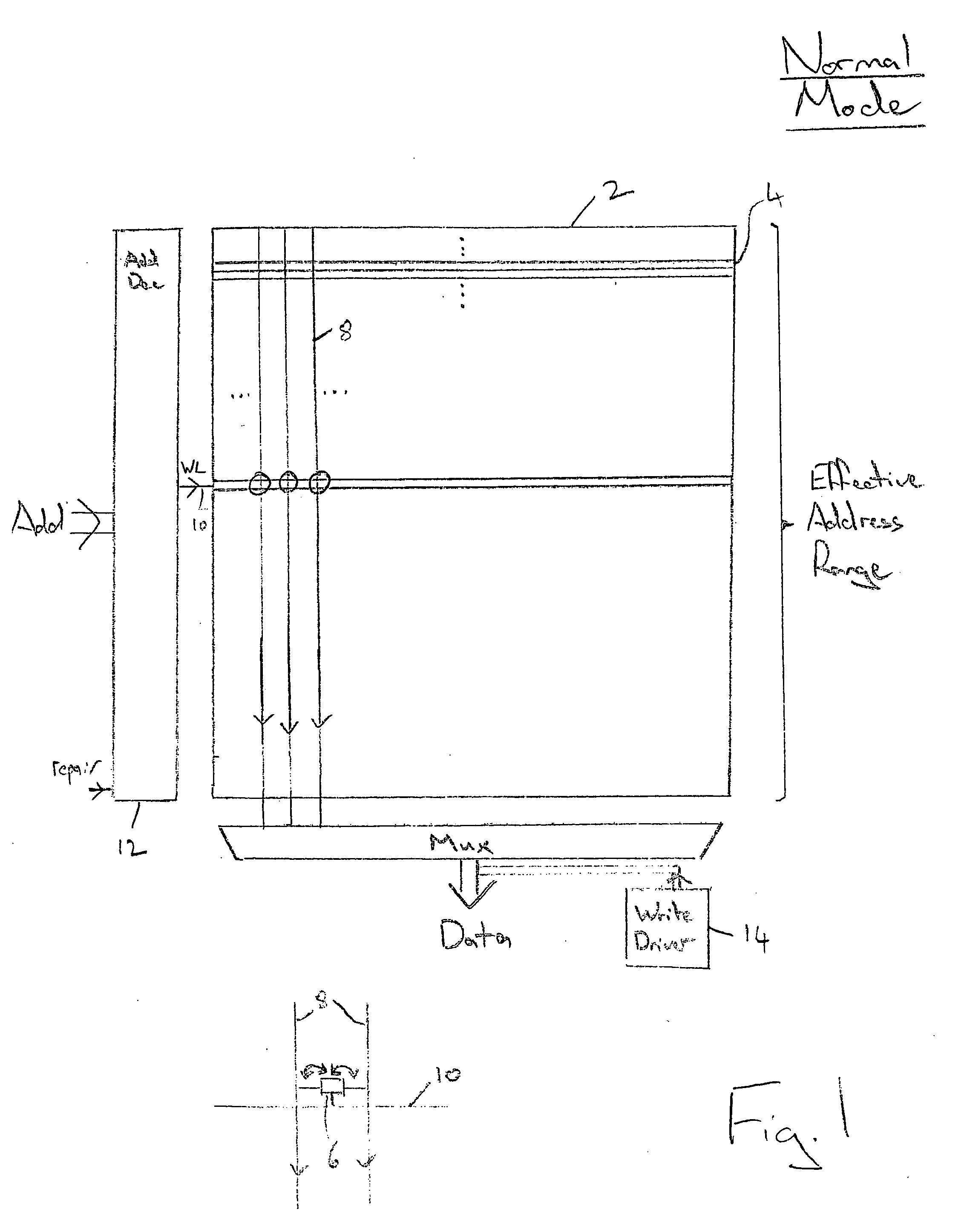
[0045]FIG. 1 schematically illustrates a memory array 2 comprising a plurality of rows of memory cells 4. An individual memory cell 6 is shown in expanded form coupled to a bit line pair 8 and a word line 10. It will be appreciated that the memory array 2 can be considered to be formed of a plurality of rows of memory cells, those memory cells also lining up to form a plurality of columns of memory cells 4. The memory cells of a given column of memory cells are coupled to the same bit lines 8 which run along the column. The memory cells 6 within a row of memory cells 4 share a common word line 10. When an address decoder 12 decodes an input address (or part of such an address), it operates in a normal mode of operation to generate a single word line select signal on a single word line 10 which connects the memory cells 6 within that row with the bit lines of their respective columns. When the memory cells 6 are connected to the bit lines 8, data can be read out of the memory cell 6 ...


PUM


Abstract

A memory array 2 has an address decoder 12 responsive to a repair signal to operate either in a normal mode or a repair mode. In the normal mode a data bit is stored within a single memory cell 6. In the repair mode a data bit is stored within multiple memory cells 6 of a common column of memory cells sharing bit lines 8. This provides increased defect resistance when operating in the repair mode at the cost of reduced memory capacity.

Description

BACKGROUND OF THE INVENTION[0001]1. Field of the Invention[0002]This invention relates to the field of memory arrays within integrated circuits. More particularly, this invention relates to the repair of defective circuits within memory arrays.[0003]2. Description of the Prior Art[0004]It is know to provide memory arrays with repair circuits which seek compensate for defective circuit elements within those memory arrays. As an example, it is known to provide redundant column and redundant row circuitry whereby, if a column or a row is defective, then it can be functionally substituted with a redundant column or a redundant row. Whilst these techniques are effective in improving the yield of useable integrated circuits, they suffer from the disadvantage of requiring additional circuit area overhead to provide the redundant columns and rows. Furthermore, a finite number such redundant columns may be provided and, if the number of defective rows or columns exceeds the number of redunda...

Claims


Application Information

Patent Timeline
Patent Type & Authority Applications(United States)
IPC IPC(8): G11C8/12G11C8/00
CPCG11C8/10G11C29/846G11C29/844G11C29/74
Inventor MITTAL, ANURAGKWON, JUNGTAE
Owner ARM LTD
Why Eureka
Try Eureka