Method of fabricating dual damascene structure

Active Publication Date: 2008-07-17
UNITED MICROELECTRONICS CORP
View PDF9 Cites 22 Cited by
  • Summary
  • Abstract
  • Description
  • Claims
  • Application Information

AI Technical Summary

Benefits of technology

[0010]Accordingly, this invention provides a method of fabricating a dual damascene structure that can prevent rou

Problems solved by technology

However, copper is difficult to etch, so that a Cu-interconnect structure is usually f

Method used


Image

  • Method of fabricating dual damascene structure
  • Method of fabricating dual damascene structure
  • Method of fabricating dual damascene structure

Examples


first embodiment

[0034]FIGS. 3A-3F illustrate, in a cross-sectional view, a process flow of fabricating a dual damascene structure according to the first embodiment of this invention.

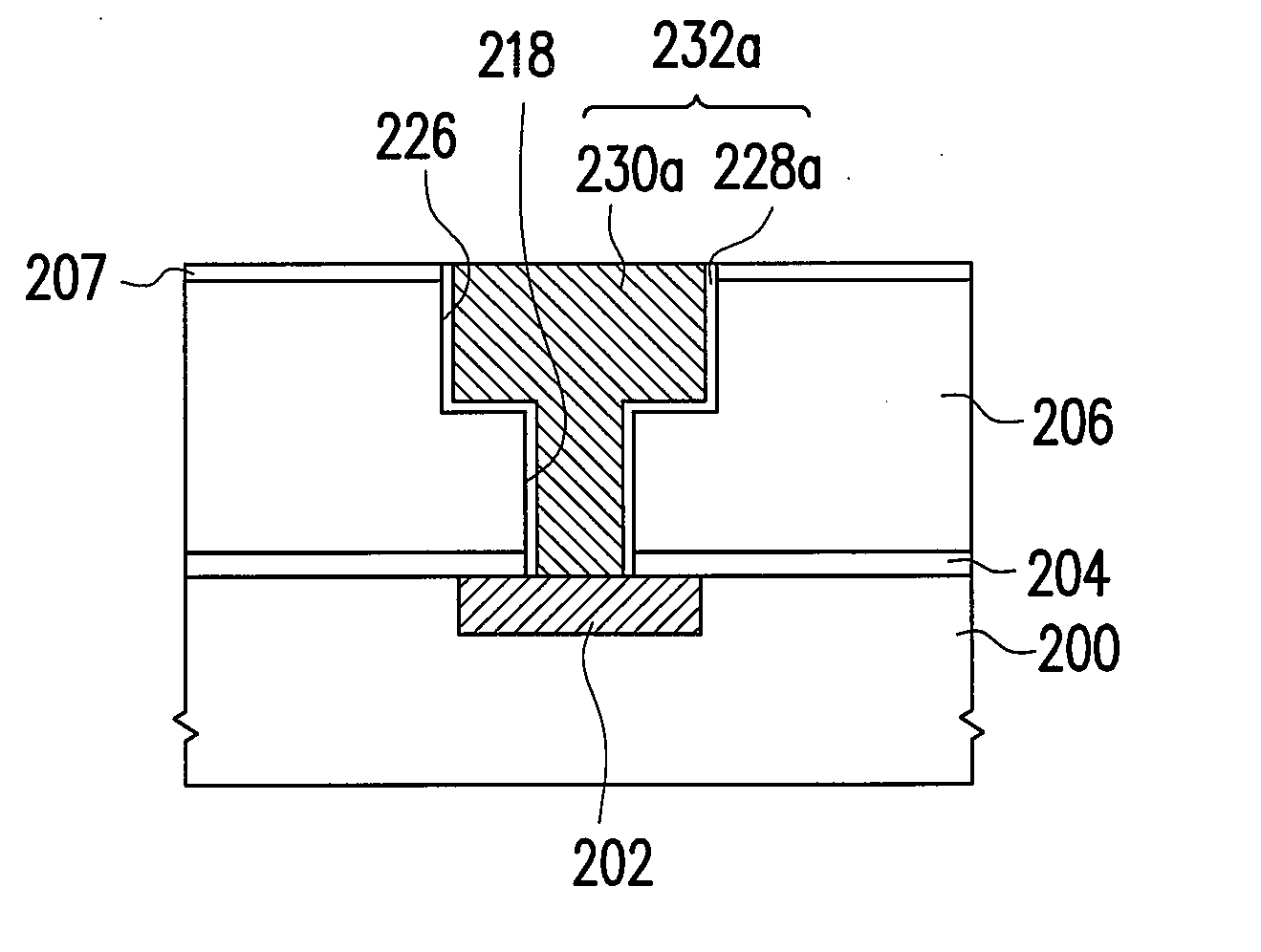
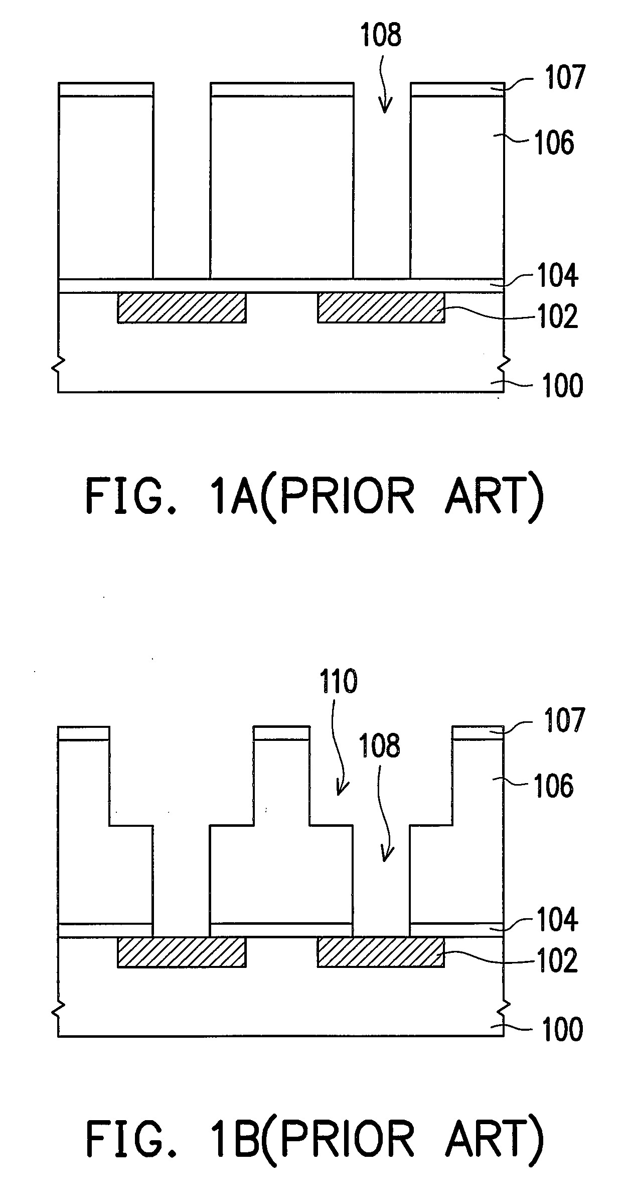
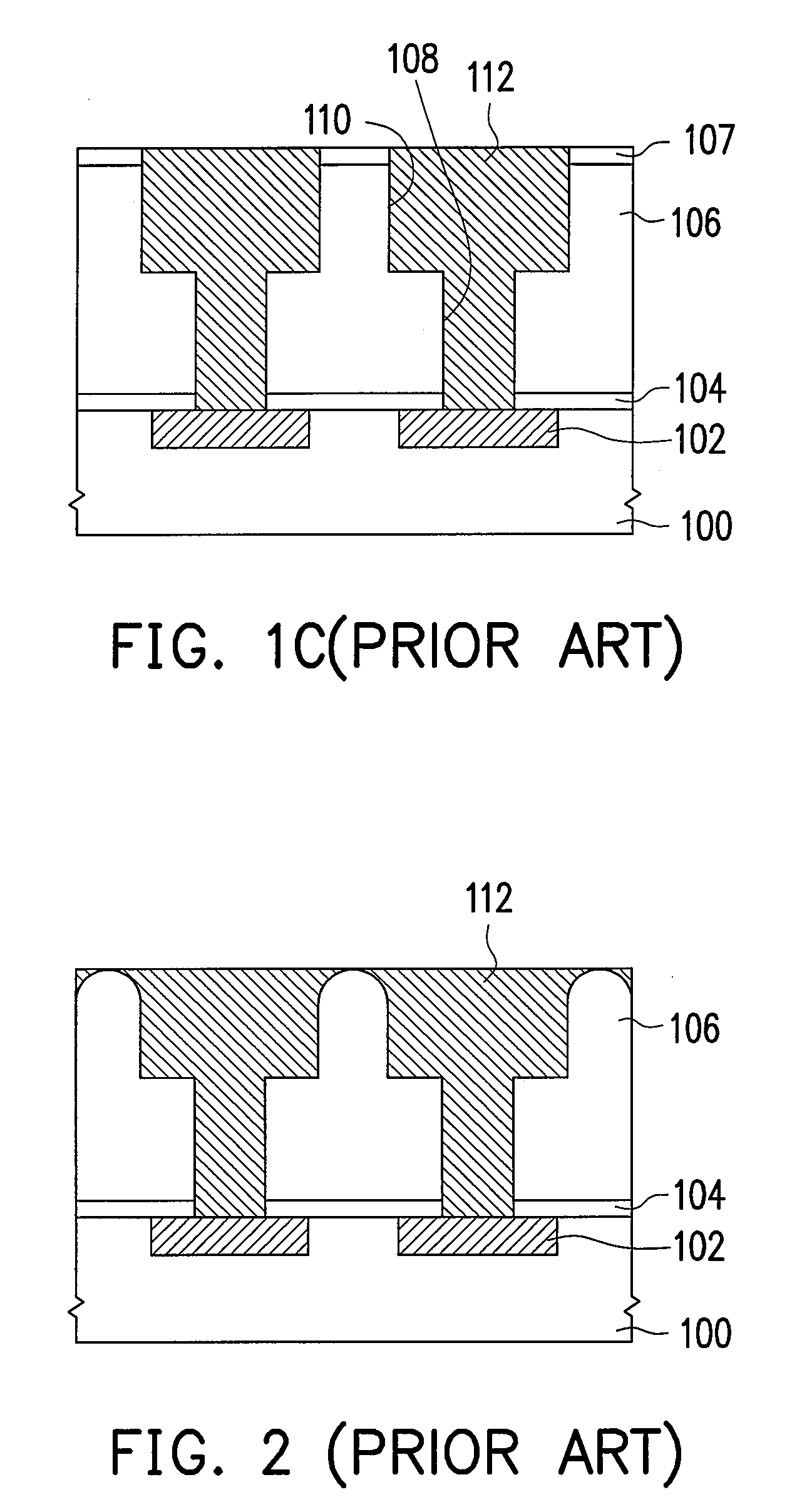
[0035]Referring to FIG. 3A, a substrate 200 having a conductive layer 202 and a liner layer 204 thereon is provided, possibly being a semiconductor substrate like a bulk-Si substrate or an SOI substrate. The conductive layer 202 may be a metal interconnect like a Cu line. The liner layer 204 can prevent oxidation of the conductive layer 202, and may be an SiN layer. A dielectric layer 206, such as a low-k layer with a dielectric constant smaller than 4, is formed on the liner layer 204. A metal hard mask layer 210 is formed on the dielectric layer 206 through, for example, CVD or sputtering, possibly including a material selected from Ti, Ta, W, TiN, TaN, WN and their combinations and having a thickness of 50-300 Å. The thickness of the metal hard mask layer 210 is preferably just enough to avoid via-plug bridging, and ...

second embodiment

[0043]FIGS. 5A-5F illustrate, in a cross-sectional view, a process flow of fabricating a dual damascene structure according to the second embodiment of this invention. This process is similar to that in the first embodiment, except that after the dielectric layer is formed but before the metal hard mask layer is formed, a cap layer is formed capable of serving as a polishing stop layer in the subsequent CMP process.

[0044]Referring to FIG. 5A, a structure including a substrate 200, a conductive layer 202, a liner layer 204 and a dielectric layer 206 is formed as in the first embodiment, while the materials and forming methods of the layers may also be the same. A cap layer 206 is formed on the dielectric layer 206 through, for example, CVD, possibly including SiO, SiN, SiCN, SiC or SiON. A metal hard mask layer 210 is then formed on the cap layer 208, possibly in the same manner mentioned above. In some cases, an ARC 212 is further formed on the metal hard mask layer 210. A photoresi...

third embodiment

[0050]FIGS. 6A-6F illustrate, in a cross-sectional view, a process flow of fabricating a dual damascene structure according to the third embodiment of this invention. This process is similar to that in the first embodiment, except that after the metal hard mask layer is formed but before the ARC is formed, a cap layer is formed on the metal hard mask layer to prevent the same from being exposed and causing contamination in the step of removing the liner layer exposed in the via hole.

[0051]Referring to FIG. 6A, a structure including a substrate 200, a conductive layer 202, a liner layer 204, a dielectric layer 206 and a metal hard mask layer 210 is formed as in the first embodiment, while the materials and forming methods of the layers may also be the same. A cap layer 206 is formed on the hard mask layer 210, possibly in the same manner mentioned above. In some cases, an ARC 212 is further formed on the cap layer 208. A photoresist layer 214 is then formed on the substrate 200, with...


PUM


Abstract

A method of fabricating a dual damascene structure is described. A dielectric layer and a metal hard mask layer are sequentially formed on a substrate having thereon a conductive layer and a liner layer. The metal hard mask layer and the dielectric layer are patterned to form a via hole exposing a portion of the liner layer. A gap-filling layer is filled in the via hole, having a height of ¼ to ½ of the depth of the via hole. A trench is formed in the metal hard mask layer and the dielectric layer. The gap-filling layer is removed to expose the portion of the liner layer, which is then removed. A metal layer is formed filling in the via hole and the trench, and then the metal hard mask layer is removed.

Description

BACKGROUND OF THE INVENTION[0001]1. Field of Invention[0002]The present invention relates to an integrated circuit (IC) interconnect process, and more particularly to a method of fabricating a dual damascene structure.[0003]2. Description of Related Art[0004]As the integration degree of semiconductor device is increased, multilevel metal interconnect is used widely. When the resistance of the metal of a metal interconnect is lower, the reliability and the performance of the device are generally higher. Since copper has a relatively low resistance among various metal materials, it is suitably used in a multilevel metal interconnect. However, copper is difficult to etch, so that a Cu-interconnect structure is usually formed with a dual damascene process.[0005]In a dual damascene process, a trench and a via hole are formed in a dielectric layer, and then metal is filled in them to form a metal line and a via plug. FIGS. 1A-1C illustrate a process flow of fabricating a dual damascene st...

Claims


Application Information

Patent Timeline
IPC IPC(8): H01L21/768
CPCH01L21/76808H01L21/31144
Inventor CHANG, KUANG-YEHMA, HONG
Owner UNITED MICROELECTRONICS CORP
Why Eureka
Try Eureka