
Dielectric cap having material with optical band gap to substantially block UV radiation during curing treatment, and related methods

Inactive Publication Date: 2008-07-24
GLOBALFOUNDRIES INC
View PDF9 Cites 22 Cited by
  • Summary
  • Abstract
  • Description
  • Claims
  • Application Information

AI Technical Summary

Benefits of technology

[0010]A dielectric cap and related methods are disclosed. In one embodiment, the dielectric cap includes a dielectric material having an optical band gap (e.g., greater than about 3.0 electron-Volts) to substantially block ultraviolet radiation during a curing treatment, and including nitrogen with electron donor, double bond electrons. The dielectric cap exhibits a high modulus and is stable under post ULK UV curing treatments for, for example, copper low k backend-of-line (BEOL) nanoelectronic devices, leading to less film and device cracking and improved reliability.

Problems solved by technology

While aluminum-based metallurgies have been the material of choice for use as metal interconnects in the past, aluminum no longer satisfies the requirements as circuit density and speeds for IC chips increase and the scale of devices decreases to nanometer dimensions.
One challenge relative to using copper is that it diffuses readily into the surrounding dielectric material as processing steps continue.
This post cure UV radiation, for example, causes increasing stress in the cap layer and causes cracking in both the cap layer and the ULK layers, Any crack in the cap layer may lead to copper diffusion into the ILD layer through the seam leading to formation of a copper nodule under the cap layer.
Such a copper nodule may lead to short circuits due to leakage of current between adjacent interconnect lines, UV and / or E-beam radiation may also cause other damages such as increased stress, delamination and blister formation over patterned copper lines, particularly during subsequent dielectric depositions, metallization, and chemical-mechanical polishing.

Method used


Image

  • Dielectric cap having material with optical band gap to substantially block UV radiation during curing treatment, and related methods
  • Dielectric cap having material with optical band gap to substantially block UV radiation during curing treatment, and related methods

Examples


Embodiment Construction

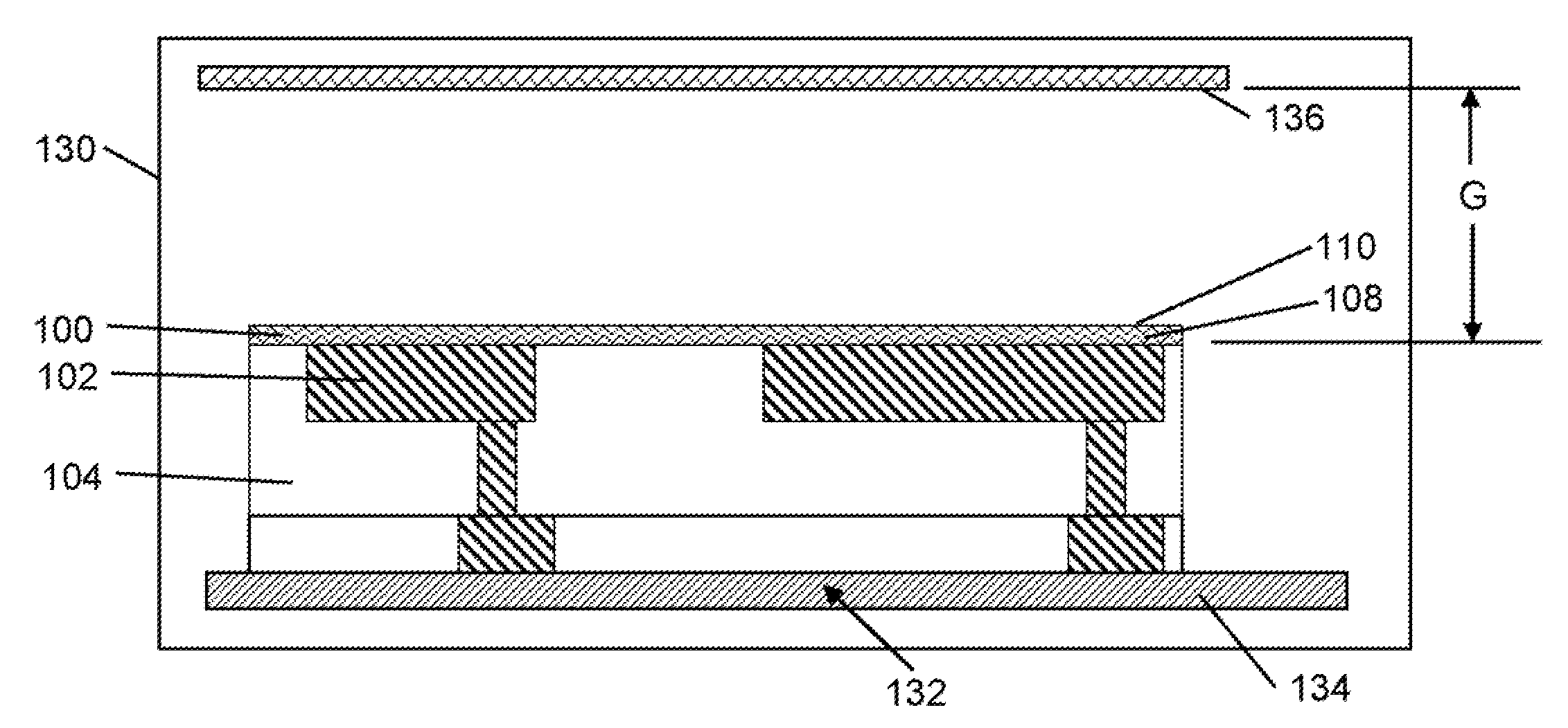
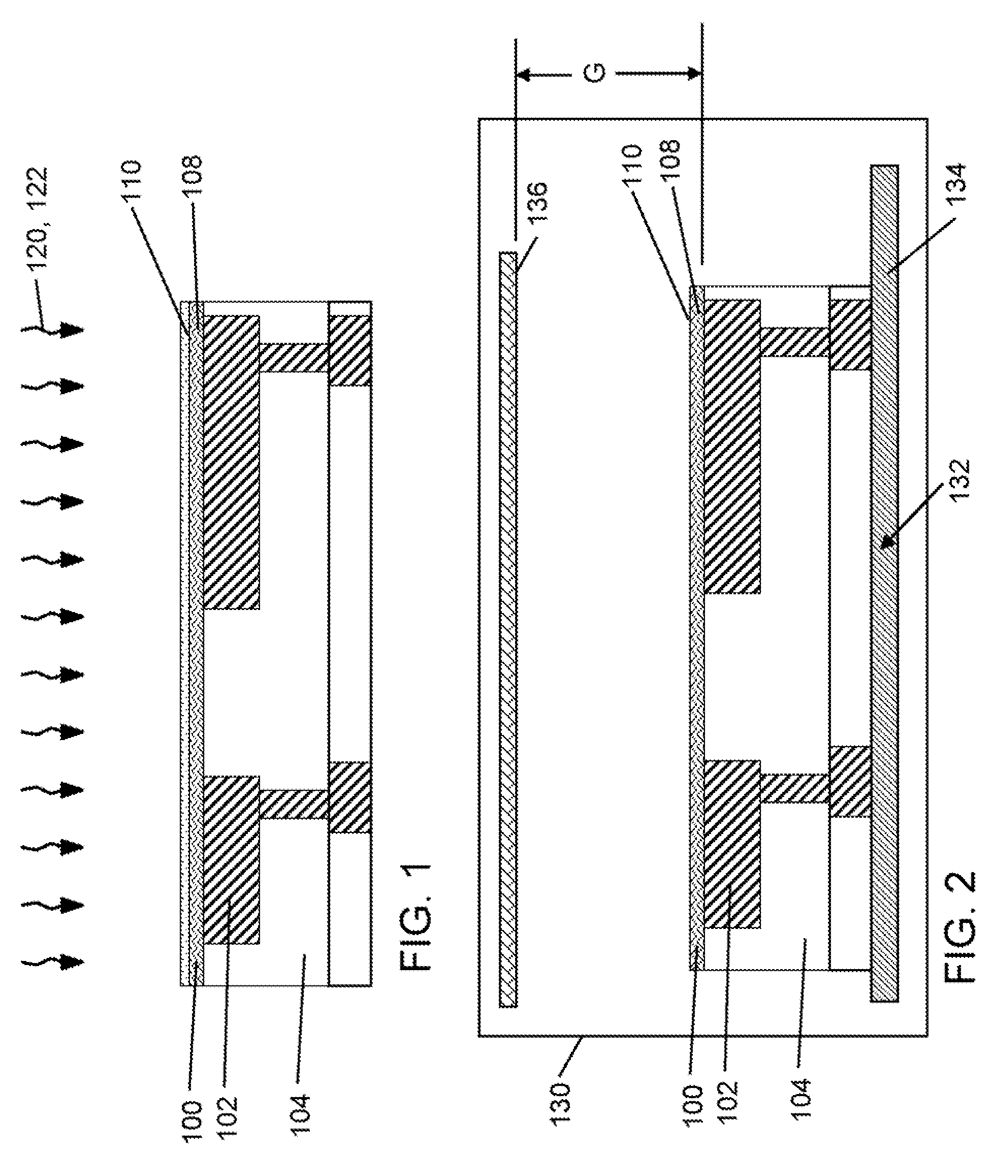
[0019]Referring to FIG. 1, a dielectric cap 100 and related methods are disclosed. Dielectric cap 100 is used in interconnect structures in ultra-large scale integrated (ULSI) nano and microelectronic integrated circuit (IC) chips including, for example, high speed microprocessors, application specific integrated circuits, memory storage devices, and related electronic structures with a multilayered barrier layer. Dielectric caps, in general, are very stable capping barrier layers used for, among other things, protecting interconnect-metallization in back-end-o-line (BEOL) structures under ultraviolet (UV) and / or E-beam radiation curing treatments.

[0020]Dielectric cap 100 may be formed, for example, over a conductor 102 such as copper (Cu) or aluminum (Al) in an inter-level dielectric (ILD) 104. ILD 104 may include any now known or later developed ultra low dielectric constant (ULK) material such as porous hydrogenated silicon oxycarbide (pSiCOH), spin-on low k dielectrics including...


PUM


Abstract

A dielectric cap and related methods are disclosed. In one embodiment, the dielectric cap includes a dielectric material having an optical band gap (e.g. greater than about 3.0 electron-Volts) to substantially block ultraviolet radiation during a curing treatment, and including nitrogen with electron donor, double bond electrons. The dielectric cap exhibits a high modulus and is stable under post ULK UV curing treatments for, for example: copper low k back-end-of-line (BEOL) nanoelectronic devices, leading to less film and device cracking and improved reliability,

Description

BACKGROUND OF THE INVENTION[0001]1. Technical Field[0002]The invention relates generally to integrated circuit (IC) chip fabrication, and more particularly, to a dielectric cap for ultra low dielectric constant (ULK) inter-level dielectrics.[0003]2. Background Art[0004]In traditional IC chips, aluminum and aluminum alloys have been used as interconnect metallurgies for providing electrical connections to and from devices in back-end-of-line (BEOL) layers of the devices. While aluminum-based metallurgies have been the material of choice for use as metal interconnects in the past, aluminum no longer satisfies the requirements as circuit density and speeds for IC chips increase and the scale of devices decreases to nanometer dimensions. Thus, copper is being employed as a replacement for aluminum because of its lower resistivity and its lower susceptibility to electromigration failure as compared to aluminum.[0005]One challenge relative to using copper is that it diffuses readily into ...

Claims


Application Information

Patent Timeline
IPC IPC(8): H01L23/58H01L21/318
CPCH01L21/318H01L21/3185H01L21/76826H01L21/76828H01L21/76834H01L21/02274H01L21/02123H01L21/02126H01L21/02167H01L21/0217H01L21/02348H01L21/77B82Y40/00
Inventor BELYANSKY, MICHAEL P.BONILLA, GRISELDALIU, XIAO HUNGUYEN, SON VANSHAW, THOMAS M.SHOBHA, HOSADURGA K.YANG, DAEWON
Owner GLOBALFOUNDRIES INC
Learn More