Measuring instrument and laser beam machine for wafer

a laser beam machine and measuring instrument technology, applied in the field of measuring instruments, can solve the problems of low productivity and inability to form uniform degenerated layers, and achieve the effect of reliably measuring the thickness or the height of the upper face of the wafer

Active Publication Date: 2008-07-31
DISCO CORP
View PDF2 Cites 17 Cited by
  • Summary
  • Abstract
  • Description
  • Claims
  • Application Information

AI Technical Summary

Benefits of technology

[0010]Therefore, it is an object of the present invention to provide a measuring instrument for a wafer which can reliably measure the thickness or the height of an upper face of a...

Problems solved by technology

However, the via hole formed in the semiconductor wafer is as small as 100 to 300 μm in diameter, and perforation by drilling has a problem that the productivity is low.
However, if the semiconductor wa...

Method used


Image

  • Measuring instrument and laser beam machine for wafer
  • Measuring instrument and laser beam machine for wafer
  • Measuring instrument and laser beam machine for wafer

Examples


Embodiment Construction

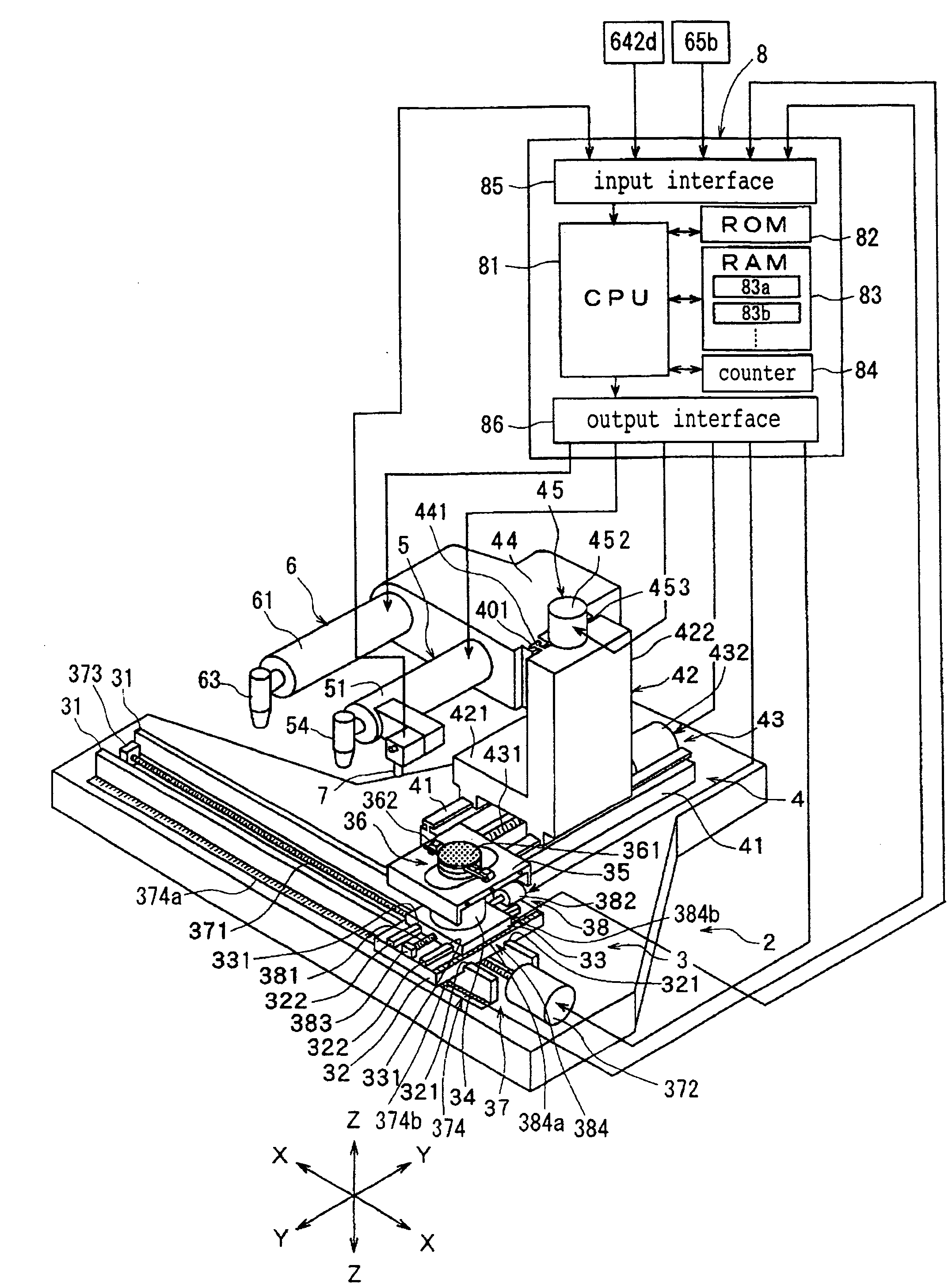
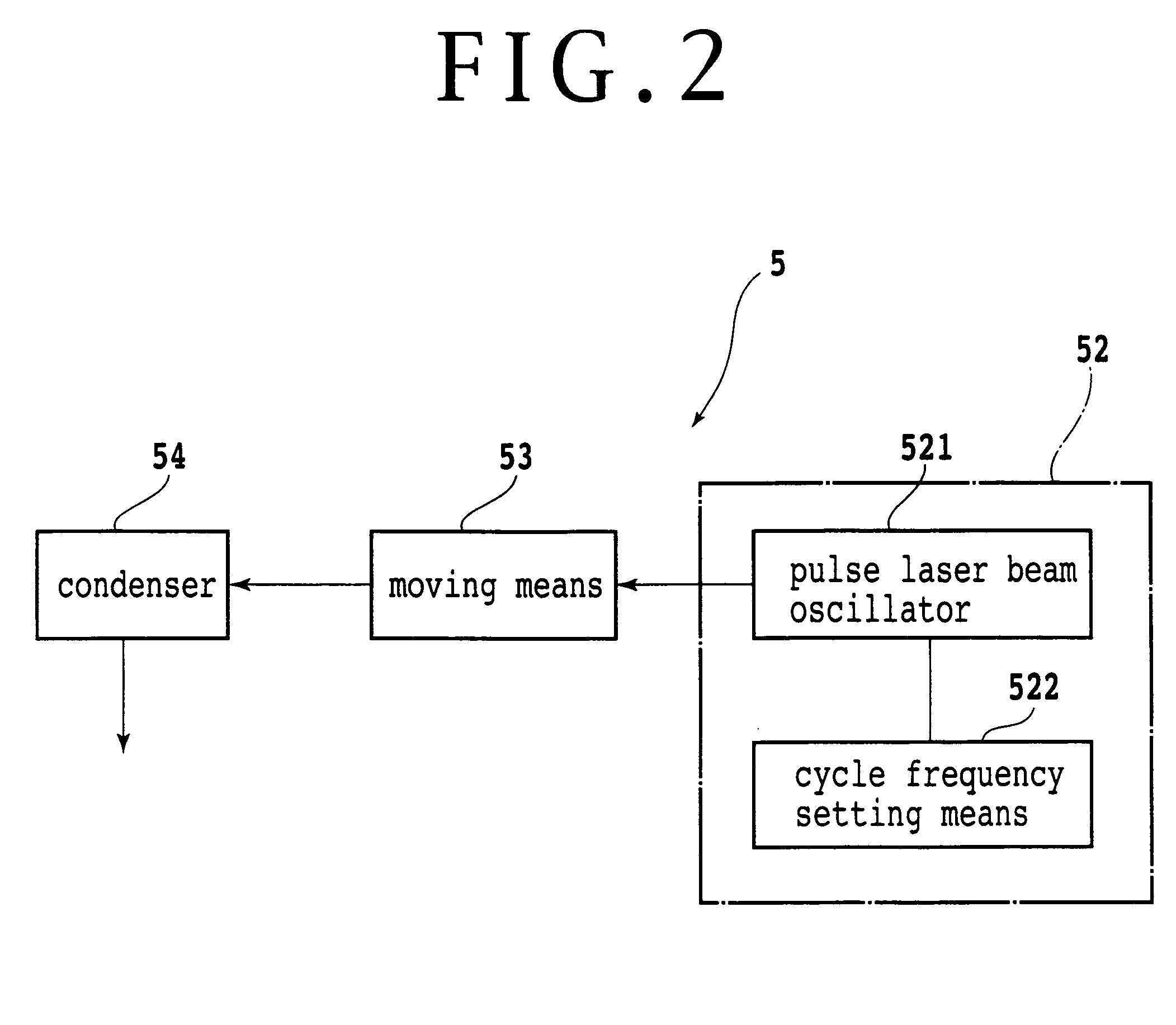
[0034]In the following, a measuring instrument and a laser beam machine or laser processing machine for a wafer according to the preferred embodiments of the present invention are described in detail with reference to the accompanying drawings. FIG. 1 shows a perspective view of a laser beam machine configured in accordance with the present invention. Referring to FIG. 1, the laser beam machine shown includes a stationary base 2, a chuck table mechanism 3 disposed for movement in a workpiece feeding direction (X-axis direction) indicated by an arrow mark X for holding a workpiece thereon, a laser beam irradiation unit supporting mechanism 4 disposed for movement in an indexing direction (Y-axis direction) indicated by an arrow mark Y and perpendicular to the workpiece feeding direction (X-axis direction) indicated by the arrow mark X on the stationary base 2, a machining laser beam irradiation unit 5 disposed for movement in a direction (Z-axis direction) indicated by an arrow mark ...


PUM


Abstract

A measuring instrument for a wafer for measuring the thickness of a wafer held on a chuck table using a laser beam includes a condenser for condensing and irradiating the laser beam on the wafer held on the chuck table, a light reception unit for receiving reflected light of the laser beam irradiated upon the wafer, a convergence light point changing unit for changing the convergence light point of the laser beam, and a control unit for measuring the thickness of the wafer based on a change signal from the convergence light point changing unit and a light reception signal from the light reception unit. The control unit stores a thickness control map. The control unit controls an angle adjustment actuator, provided for adjusting the installation angle of a pair of mirrors, to change the installation angle and detects two peaks of the light amount based on the reception signal from the light reception unit.

Description

BACKGROUND OF THE INVENTION[0001]1. Field of the Invention[0002]This invention relates to a measuring instrument for measuring the thickness or the height of an upper face of a wafer such as a semiconductor wafer held on a chuck table equipped on a processing machine for a wafer such as a laser beam machine or laser processing machine.[0003]2. Description of the Related Art[0004]In a semiconductor device fabrication process, a plurality of regions are partitioned by scheduled division lines called streets disposed in grating-like arrangement on the surface of a semiconductor wafer having a substantially disk shape, and such a device as an IC or an LSI is formed in each of the partitioned regions. Then, the semiconductor wafer is cut along the streets to cut the regions in which the devices are formed to divide individual semiconductor chips.[0005]In order to achieve down-scaling and enhancement in function of an apparatus, a module structure wherein a plurality of semiconductor chip...

Claims


Application Information

Patent Timeline
IPC IPC(8): G01B11/06B23K26/03G01B11/02H01L21/66
CPCB23K26/048G01B11/0625B23K2201/40B23K26/0861B23K2101/40
Inventor SAWABE, TAIKINOMARU, KEIJI
Owner DISCO CORP
Why Eureka
Try Eureka