Method of forming a metal layer over a patterned dielectric by electroless deposition using a selectively provided activation layer

a dielectric and activation layer technology, applied in the field of integrated circuits, can solve the problems of ineffective patterned dielectric by the usual employed anisotropic, copper also exhibits, and cannot be efficiently applied onto the substrate in large amounts, and achieves a high degree of selectivity, high reliability of bottom-to-top fill behavior, and reduced pinch-off effects at upper portions of the opening.

Inactive Publication Date: 2008-07-31
GLOBALFOUNDRIES INC
View PDF86 Cites 16 Cited by
  • Summary
  • Abstract
  • Description
  • Claims
  • Application Information

AI Technical Summary

Benefits of technology

[0010]Generally, the subject matter disclosed herein addresses the problems encountered in conventional process regimes with respect to forming metal-containing regions in advanced semiconductor devices in that efficient electroless deposition processes may be used for filling the corresponding openings with a high degree of selectivity, without requiring respective current distribution layers as is the case in electroplating processes. Since typically an electrochemical process without external current flow may require an activation energy or a corresponding catalyst or nucleation material, a respective material may be selectively provided on the surface areas of openings, at which a corresponding deposition of the metal-containing material is desired. That is, the bottom of a respective opening may receive, or may have an exposed surface of, a corresponding activation material or a catalyst material in a highly selective manner, thereby providing the possibility of substantially determining the growth direction in the subsequent electrochemical deposition process and accomplishing a highly reliable bottom-to-top fill behavior. Furthermore, since the corresponding catalyst material may be provided in a highly selective manner, any pinch-off effects at upper portions of the opening may be significantly reduced, thereby resulting in enhanced fill capability, which may allow further device scaling required in future device generations. Furthermore, the provision of substantially a single growth direction during the electrochemical deposition process may provide the possibility of efficiently controlling the resulting crystallinity of the metal-containing material without complex post-deposition treatments.

Problems solved by technology

Due to the large number of circuit elements and the required complex layout of advanced integrated circuits, generally the electrical connection of the individual circuit elements may not be established within the same level on which the circuit elements are manufactured, but requires one or more additional “wiring” layers, also referred to as metallization layers.
Since the fabrication of a plurality of metallization layers entails extremely challenging issues to be solved, such as mechanical, thermal and electrical reliability of several stacked metallization layers that are required, for example, for sophisticated microprocessors, semiconductor manufacturers are increasingly replacing the well-established materials, such as aluminum, with a metal that allows higher current densities and hence allows a reduction in the dimensions of the interconnections.
In spite of these advantages, copper also exhibits a number of disadvantages regarding the processing and handling of copper in a semiconductor facility.
For instance, copper may not be efficiently applied onto a substrate in larger amounts by well-established deposition methods, such as chemical vapor deposition (CVD) and physical vapor deposition (PVD), and also may not be effectively patterned by the usually employed anisotropic etch procedures due to copper's characteristics to form non-volatile reaction products.
However, for completely filling respective openings, such as contact openings, vias, trenches and the like, in a reliable and substantially void-free manner, complex deposition techniques may be required, wherein, for instance, in well-established techniques for forming copper-based metallization layers, an electroplating process may be used for obtaining a substantially bottom-to-top fill behavior, where the copper material is substantially deposited from bottom to top followed by a removal of any excess material on the basis of chemical mechanical polishing (CMP) and / or electrochemical etch processes.
Furthermore, the electroplating process may require highly complex chemistries, since, in high aspect openings, the deposition process may also proceed at sidewall portions of the respective opening due to the presence of the corresponding currents distribution layer at all exposed surfaces, which may result in a pinch-off at the upper portion of the opening prior to completely filling the remaining volume of the opening, unless complex current pulse patterns in combination with sensitive additives are used for significantly increasing the vertical growth rate compared to the horizontal growth rate.
Furthermore, the different growth directions, although occurring in very different growth rates, and the complex chemistries, used in the above-mentioned complex compensation mechanisms, may result in non-desired crystallinity, i.e., grain structure, of the resulting metal structure, thereby also requiring complex post-deposition treatments in order to provide the desired crystallinity and texture of the resulting metal structure.
Consequently, with every new device generation, requiring even further reduced cross-sections of the respective interconnect structures, even further restrictive requirements may have to be fulfilled, since increased current densities may require enhanced electromigration behavior of the corresponding interconnect structures.

Method used


Image

  • Method of forming a metal layer over a patterned dielectric by electroless deposition using a selectively provided activation layer
  • Method of forming a metal layer over a patterned dielectric by electroless deposition using a selectively provided activation layer
  • Method of forming a metal layer over a patterned dielectric by electroless deposition using a selectively provided activation layer

Examples


Embodiment Construction

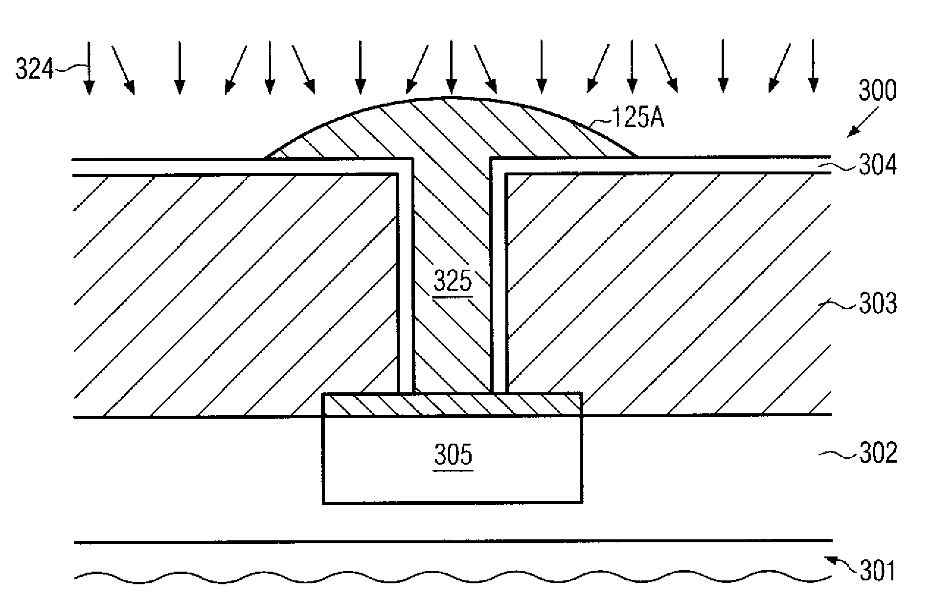
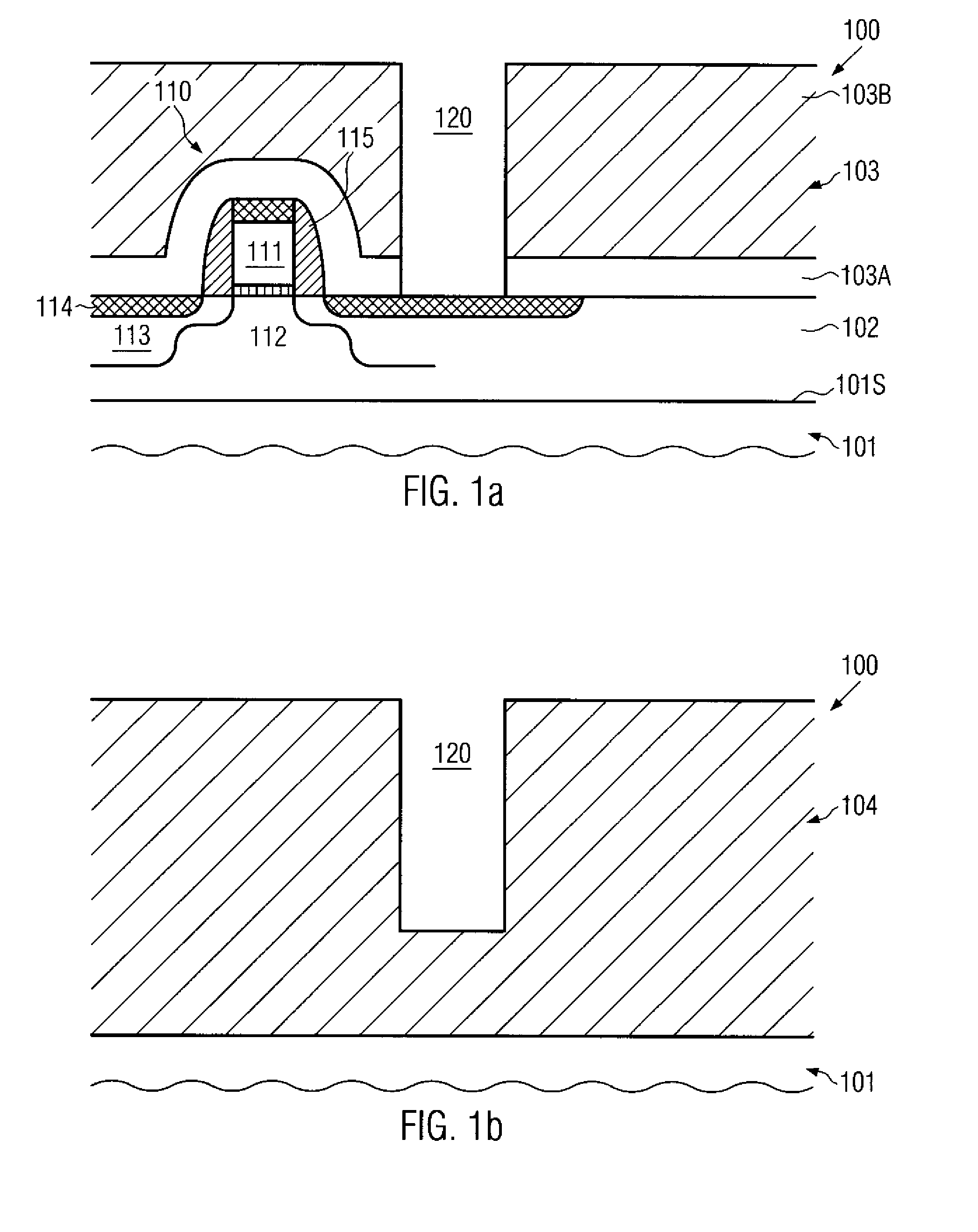
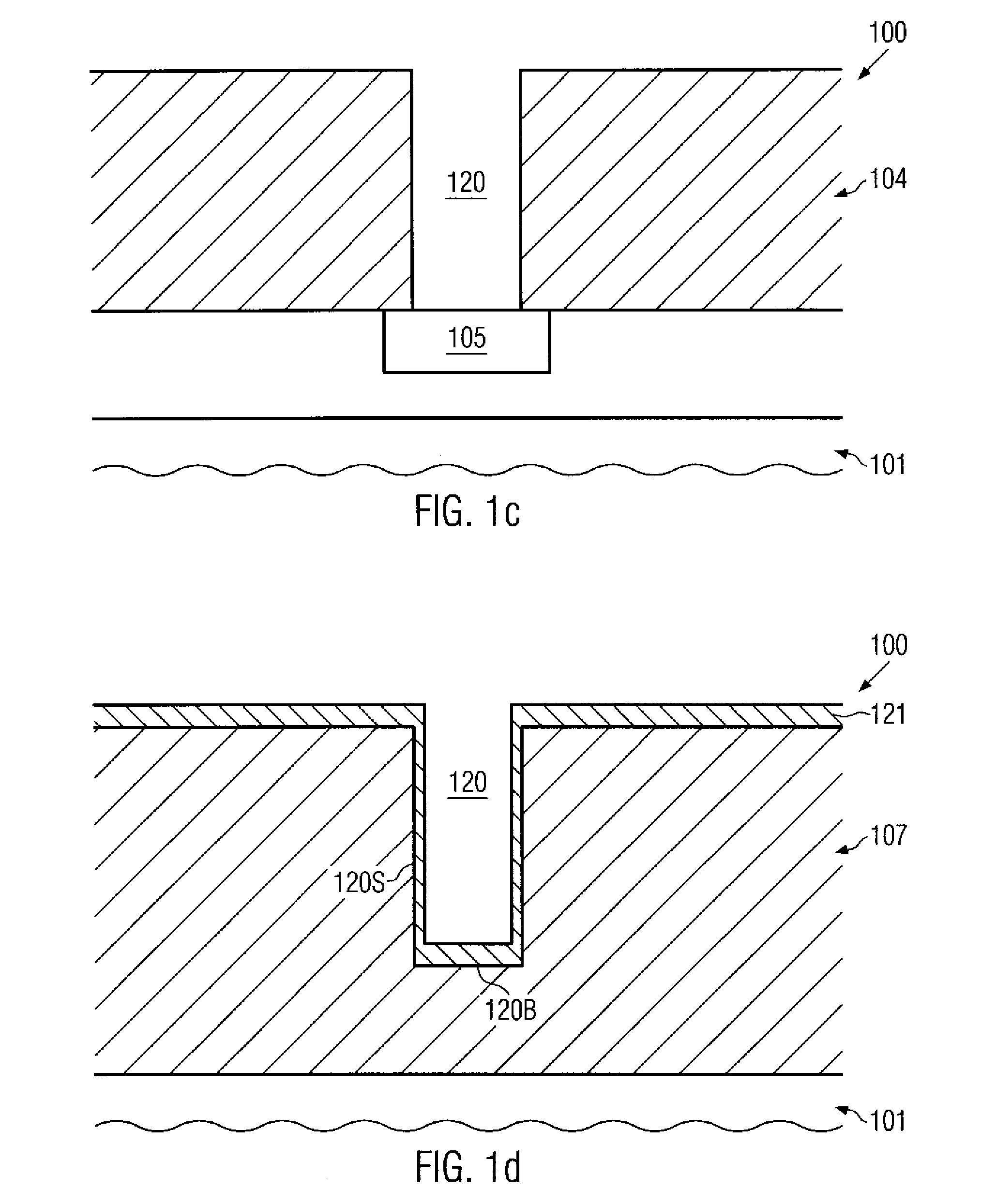
[0022]Various illustrative embodiments of the invention are described below. In the interest of clarity, not all features of an actual implementation are described in this specification. It will of course be appreciated that in the development of any such actual embodiment, numerous implementation-specific decisions must be made to achieve the developers' specific goals, such as compliance with system-related and business-related constraints, which will vary from one implementation to another. Moreover, it will be appreciated that such a development effort might be complex and time-consuming, but would nevertheless be a routine undertaking for those of ordinary skill in the art having the benefit of this disclosure.

[0023]The present subject matter will now be described with reference to the attached figures. Various structures, systems and devices are schematically depicted in the drawings for purposes of explanation only and so as to not obscure the present disclosure with details ...


PUM

PropertyMeasurementUnit
diameteraaaaaaaaaa
aspect ratioaaaaaaaaaa
lengthaaaaaaaaaa

Abstract

By forming an activation / nucleation layer selectively at a bottom of an opening, efficient electroless deposition techniques may be used for forming contacts, vias and trenches of advanced semiconductor devices. By selectively providing the activation material, a self-aligned bottom-to-top fill behavior may be obtained.

Description

BACKGROUND OF THE INVENTION[0001]1. Field of the Invention[0002]The present disclosure generally relates to the field of integrated circuits, and, more particularly, to the formation of metal layers over a patterned dielectric material, such as trenches and vias, contact plugs and the like, by a wet chemical deposition process, such as electroless plating.[0003]2. Description of the Related Art[0004]In an integrated circuit, a large number of circuit elements, such as transistors, capacitors, resistors and the like, are formed in or on an appropriate substrate, usually in a substantially planar configuration. Due to the large number of circuit elements and the required complex layout of advanced integrated circuits, generally the electrical connection of the individual circuit elements may not be established within the same level on which the circuit elements are manufactured, but requires one or more additional “wiring” layers, also referred to as metallization layers. These metall...

Claims


Application Information

Patent Timeline
Patent Type & Authority Applications(United States)
IPC IPC(8): H01L21/445
CPCH01L21/76843H01L21/76844H01L21/76849H01L21/76879H01L21/76865H01L21/76867H01L21/76874H01L21/76859
Inventor SEIDEL, ROBERTPREUSSE, AXELRICHTER, RALF
Owner GLOBALFOUNDRIES INC
Why Eureka
Try Eureka