Avalanche Photo Diode
a photo diode and avalanche technology, applied in the field of light receiving elements, can solve the problems of easy breakage on the surface of the mesa periphery, and achieve the effects of low dark current, high long-term reliability, and simple process
- Summary
- Abstract
- Description
- Claims
- Application Information
AI Technical Summary
Benefits of technology
Problems solved by technology
Method used
Image
Examples
first embodiment
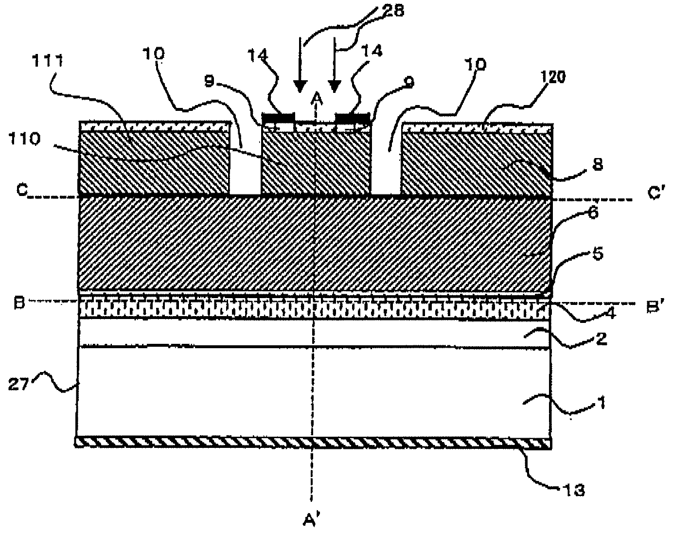
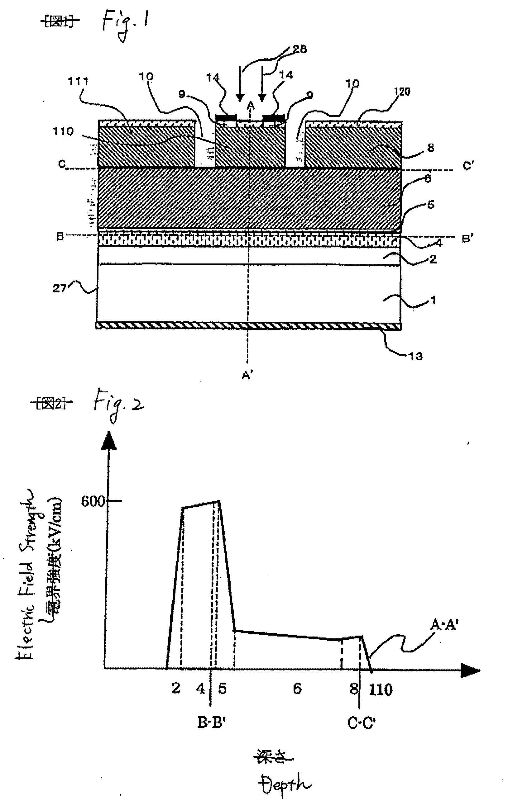
[0025]FIG. 1 is a sectional view to show the schematic structure of an avalanche photodiode according to a first embodiment of the invention. Here, n type is used as a first conduction type, p type is used as a second conduction type, an n electrode is used as a first electrode, and a p electrode is used as a second electrode. Each semiconductor layer can be manufactured using MO-CVD, a molecular beam epitaxy (MBE), etc., on a wafer-like substrate 1 of n type InP, etc., for example. In the embodiment, the semiconductor layers are manufactured according to the following step order; A first semiconductor layer 2 (which will be hereinafter referred to as buffer layer) of n type InP, etc., at a carrier density of 0.2 to 2×1019 cm−3 is grown to a thickness of 0.1 to 1 μm, an avalanche multiplication layer 4 of i type AlInAs is grown to a thickness of 0.15 to 0.4 μm, a field relaxation layer 5 of p type InP at a carrier density of 0.5 to 1×1018 cm−3 is grown to a thickness of 0.03 to 0.06...
second embodiment
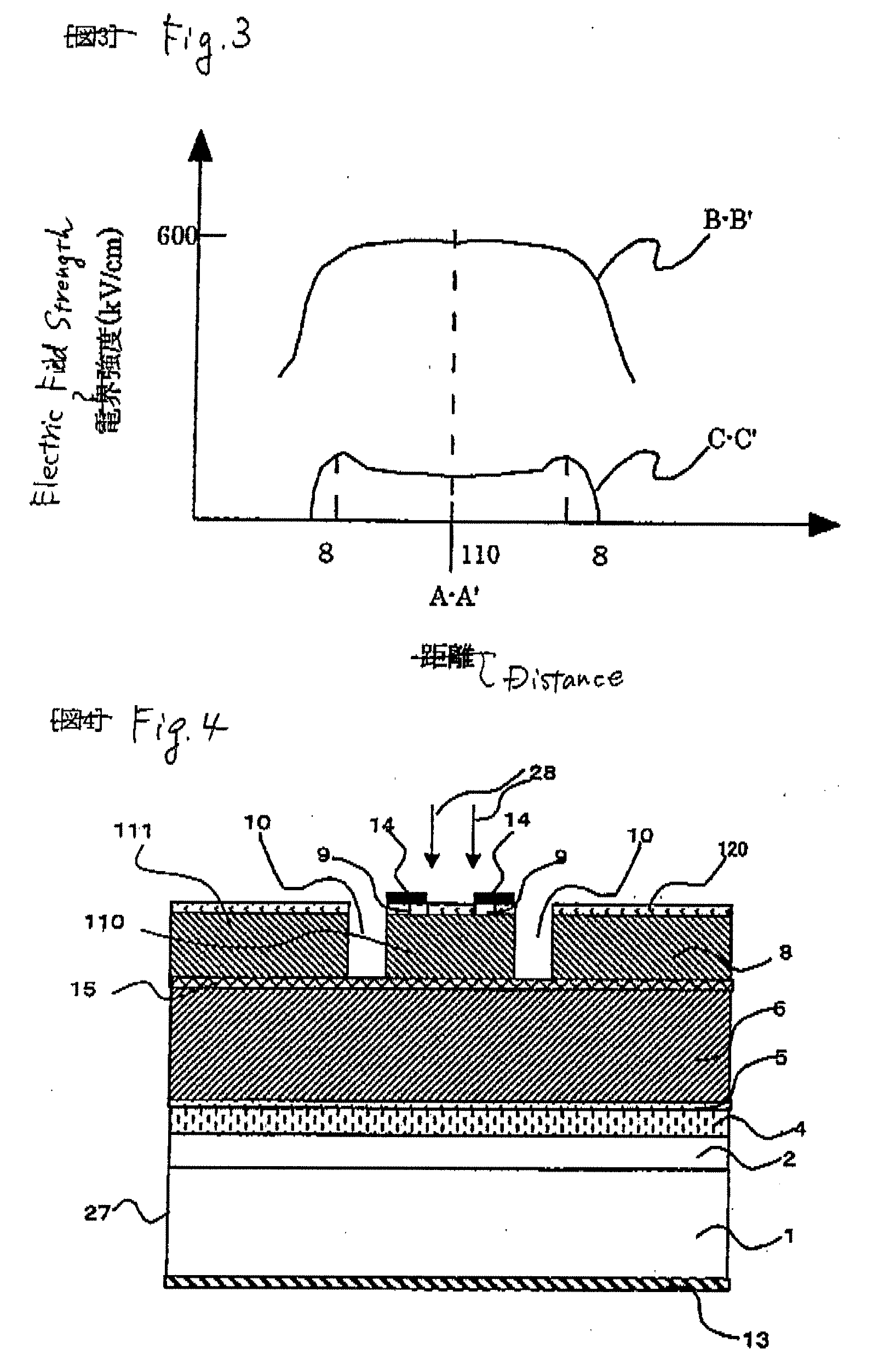
[0033]FIG. 4 is a sectional view to show a schematic structure of an avalanche photodiode according to a second embodiment of the invention. In the present embodiment, in the avalanche photodiode according to the first Embodiment, a third semiconductor layer 15 with a larger band than the light absorption layer 6 and formed of i type InP having about 0.03 μm is provided between the light absorption layer 6 and the second semiconductor layer 8, and a groove 10 is formed by leaving the third semiconductor layer 15.
[0034]According to the present embodiment, the lower portion of the groove 10 exposed to the outside can be formed with a larger band gap than the light absorption layer 6. Therefore, it is possible to achieve suppression of surface deterioration in the lower portion of the groove 10, suppression of deterioration in dark current characteristics, and improvement in durability. In addition, the region in which electric field strength thereof is partially high in the periphery ...
third embodiment
[0038]FIG. 5 is a sectional view to show a schematic structure of an avalanche photodiode according to a third embodiment of the invention. In the present embodiment, in the avalanche photodiode according to the first embodiment, an outer trench 26 is further provided in the outer periphery of the inner region 110 separated by the groove 10 and by removing up to the light absorption layer 6, for example, so that a circular region is left about 100 μm in diameter to form the side face 25.
[0039]In the present embodiment, since the avalanche photodiode has the groove 10 formed therein, a depletion region 11 is formed right under the inner region 110. The dark current occurs mainly from the light absorption layer 6 and flows through the depletion region 11 and along the side face of the element. Accordingly, when the outer trench 26 is provided in the periphery of the light absorption layer 6 surrounding the depletion region 11, it is possible to shut off the path of the dark current, t...
PUM
 Abstract
Description
Claims
Application Information


