Soi mosfet device with adjustable threshold voltage

a threshold voltage and soi mosfet technology, applied in semiconductor devices, process and machine control, instruments, etc., can solve the problems of severe power consumption constraints, critical parameters, and large power consumption, and achieve the effect of limiting leakage current and improving circuit speed

Inactive Publication Date: 2008-08-14
IBM CORP
View PDF13 Cites 36 Cited by
  • Summary
  • Abstract
  • Description
  • Claims
  • Application Information

AI Technical Summary

Benefits of technology

[0012]An object of this invention is to scale down the power supply, voltage, improve the circuit speed, and limit the leakage current simultaneously.
[0014]In accordance with this invention a device and a method of manufacture thereof are provided whereby a MOSFET device formed in an SOI structure includes a conventional gate electrode and an integral auxiliary gate. A depletion switch is formed by an auxiliary gate and a thinner region of the silicon layer located below the auxiliary gate. The depletion switch controls the connection of a body contact to the channel of the MOSFET as a function of gate voltage. The depletion switch thereby isolates the body of the MOSFET from the body contact region when the gate electrode is in the ON state with the isolation being provided by maintaining a fully depleted region under the switch formed by auxiliary portion of the gate electrode and the thinner region of the SOI region. Thus the P-well is disconnected from the body contact and is in a floating state when the MOSFET is ON. On the other hand, when the MOSFET is OFF the region of the body under the auxiliary gate is not fully depleted and the body of the FET is connected to a P-well contact region. In the OFF state, a negative body bias Vpw can be applied to the P-well contact region which is connected to the channel of the MOSFET through the depletion switch. The structure suppresses subthreshold leakage current.
[0017]In accordance with another aspect of this invention, a method is provided for forming a semiconductor device including an FET device a contact, and a switch therebetween. Form a semiconductor layer over a top surface of a dielectric layer with the semiconductor layer being divided into a contact region, an FET region having a first thickness, and a switch region having a second thickness less than the first thickness. Form a conformal gate dielectric layer covering the FET region and the switch region. Form an extended gate electrode over the gate dielectric layer including an FET gate electrode located above the FET region and an auxiliary gate electrode extending from the FET gate electrode over the switch region. Form an FET device with a source region and a drain region in the FET region juxtaposed with the gate electrode, and form a contact reaching into electrical and mechanical contact with the contact region aside from the switch and distal from the FET device, whereby the auxiliary switch gate is adapted to open and close the switch in the switch region as a function of voltage applied thereto, thereby suppressing subthreshold leakage current.

Problems solved by technology

Currently power consumption has become a great concern for those designing VLSI circuits.
The demand for portability of these systems limits their battery size which places severe constraints on the power consumption.
Even for the non-portable devices, as the sizes of transistors are scaled down, with increasing circuit speed and density the result is that the amount of power consumption has become a critical parameter.
However, the threshold voltage Vt cannot be scaled down by the same amount as the power supply voltage Vdd because of the problem of sub-threshold leakage current (Ileakage) and the low limit for the sub-threshold swing.
So, for a standard Metal Oxide Semiconductor Field Effect Transistor (MOSFET) or more generally a Metal Insulator Semiconductor Field Effect Transistor (MISFET), it is increasingly challenging to scale down the power supply voltage Vdd, to improve the circuit speed, and to limit the subthreshold leakage current (Ileakage) simultaneously.
There is one disadvantage for this device.
However, there is a significant disadvantage for this device, which is that because the gate bias Vg is connected to the body, the leakage current of forward biased p-n junction at the source increases dramatically when the supply voltage rises to a level higher than 0.7V.

Method used


Image

  • Soi mosfet device with adjustable threshold voltage
  • Soi mosfet device with adjustable threshold voltage
  • Soi mosfet device with adjustable threshold voltage

Examples


Embodiment Construction

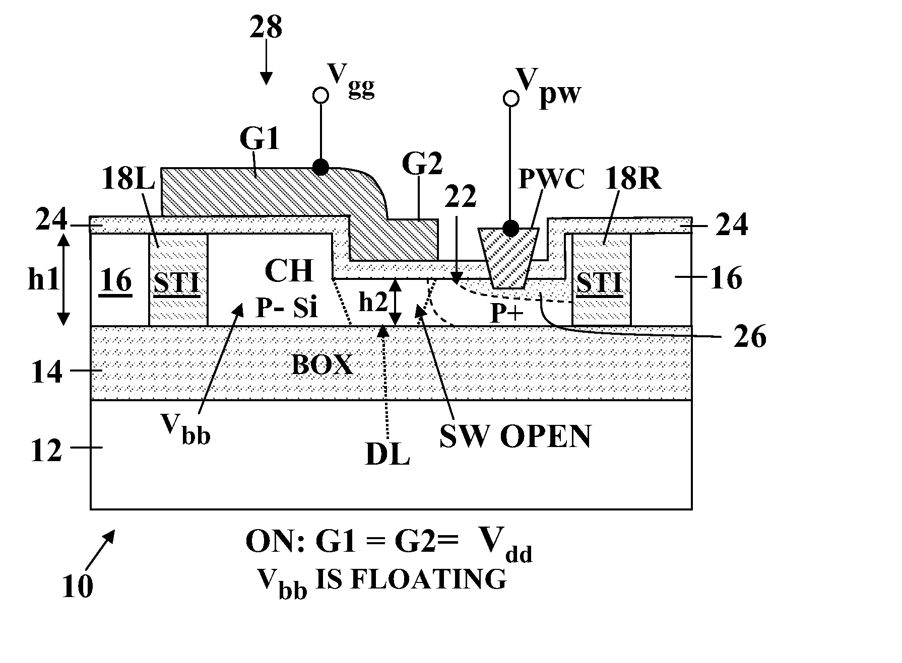
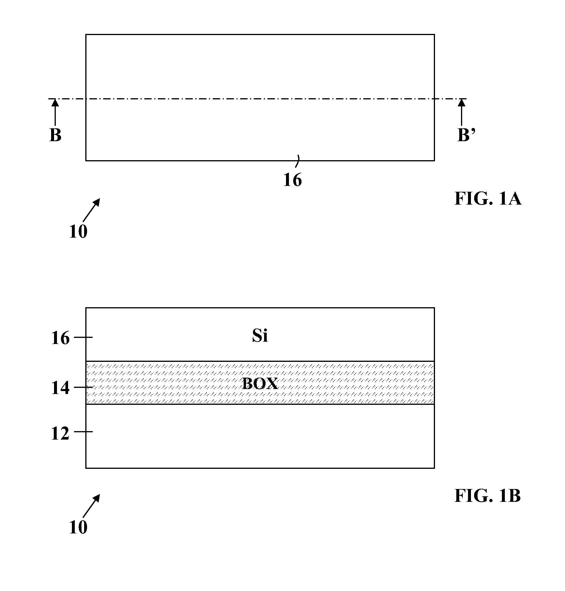
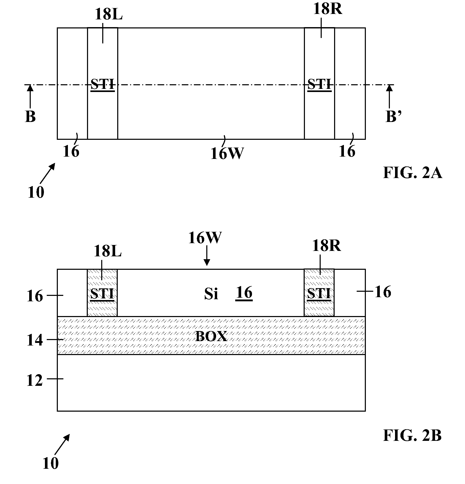
[0029]FIG. 1A shows a plan view of an early stage in the manufacturing process after step A in FIG. 12 in which an SOI NMOSFET type of MISFET semiconductor transistor device 10 has been formed in accordance with the method of this invention. FIG. 1B is a cross-sectional, elevational view of the SOI MISFET device 10 of FIG. 1A taken along line B-B′ therein. FIGS. 1A and 1B illustrate the result of performance of the step A in FIG. 12, which is to form a thick substrate 12 with a Buried Oxide (BOX) layer 14 formed thereover. In turn a thin film, monocrystalline, silicon (Si) layer 16 has been formed on the top surface of the BOX layer 14. The thin film, monocrystalline, silicon (Si) layer 16 has a thickness of “h1” which is within the conventional range of thicknesses of typical SOI silicon layers.

[0030]Referring to FIG. 1B, the MISFET device 10 is formed on the thick substrate 12 which may be composed of silicon semiconductor material or alternatively may be composed of silicon germa...


PUM


Abstract

An SOI semiconductor device includes a silicon semiconductor layer divided into an FET region with source, channel, and drain regions therein formed on a BOX layer, with a switch region next to the FET region; and a contact region next to the switch region distal from the FET region. The FET region has a greater thickness than the switch region. A conformal gate dielectric layer covers the FET region and the switch. A dual function gate electrode formed over the gate dielectric layer includes an FET portion above the FET region and an auxiliary gate portion extending therefrom above the switch region. A contact is formed reaching through the gate dielectric layer into electrical and mechanical contact with the contact region. The switch varies the depth of the depletion region to open and close current flow between the channel of the FET device and the contact region to suppress subthreshold leakage current.

Description

BACKGROUND OF THE INVENTION[0001]This invention relates to semiconductor devices and methods of manufacture thereof. More particularly this invention relates to Field Effect Transistor (FET) devices and methods of manufacture thereof.[0002]Currently power consumption has become a great concern for those designing VLSI circuits. In the past few years, many portable devices and wireless application systems have emerged and such products have become a principal driver of industry growth. The demand for portability of these systems limits their battery size which places severe constraints on the power consumption. Even for the non-portable devices, as the sizes of transistors are scaled down, with increasing circuit speed and density the result is that the amount of power consumption has become a critical parameter. To produce a satisfactory level of circuit speed it is important to maintain a sufficient level of gate over-drive voltage Vgt which is defined as gate to source voltage (Vg...

Claims


Application Information

Patent Timeline
Patent Type & Authority Applications(United States)
IPC IPC(8): G05F1/10H01L21/336
CPCH01L29/78609H01L29/66772
Inventor CHEN, XIANGDONGYANG, HAINING S.
Owner IBM CORP
Why Eureka
Try Eureka